SEMI M64 Wafer Dimensional Accuracy Testing
The SEMI M64 standard is a critical guideline in semiconductor manufacturing and testing, focusing on wafer dimensional accuracy. Semiconductor wafers are the foundation of modern electronics, and their precise dimensions ensure compatibility across various stages of production and end-use applications. SEMI M64 ensures that manufacturers maintain consistent quality by providing stringent specifications for wafer thickness, diameter, and flatness.
Wafer dimensional accuracy is paramount in ensuring that wafers meet the exacting requirements of semiconductor fabrication processes. Any deviation from these standards can lead to significant issues such as manufacturing inefficiencies, increased defect rates, and reduced product performance. This testing service ensures that each wafer adheres to SEMI M64 specifications, thereby upholding industry standards.
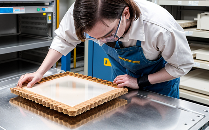
The process begins with the preparation of the wafer for testing. Typically, this involves cleaning the wafer surface to eliminate any contaminants that could interfere with accurate measurements. The wafer is then placed on a specialized fixture designed to hold it securely during measurement. High-precision instruments are used to capture data points across multiple dimensions, including thickness and diameter.
The SEMI M64 standard defines specific tolerances for these parameters. For instance, the allowable deviation in wafer diameter can range from ±0.1 mm to ±0.25 mm depending on the wafer size. Thickness variations are similarly controlled within specified limits. The flatness of the wafer is also crucial; it must be within a narrow tolerance band to ensure that subsequent processing steps proceed smoothly.
The testing equipment employed in this service includes laser interferometers and profilometers, which provide highly accurate measurements. These instruments can detect minute deviations in wafer dimensions down to fractions of a micron, ensuring compliance with SEMI M64 standards. The data collected during testing is then analyzed using advanced software tools that compare the measured values against the specified tolerances.
Once the test results are available, they are reported according to SEMI M64 guidelines. This report includes detailed metrics on wafer thickness, diameter, and flatness, along with any deviations found. Compliance reports provide a comprehensive overview of the wafer's dimensional accuracy relative to the standard, enabling manufacturers to identify areas for improvement.
Accurate testing is essential not only in semiconductor manufacturing but also in related industries that rely on precision components. By adhering to SEMI M64 standards, this testing service helps maintain industry integrity and supports continuous quality improvement efforts.
Applied Standards
| Standard Name | Description |
|---|---|
| SEMI M64-2018 | This standard defines the dimensional accuracy specifications for semiconductor wafers, including thickness, diameter, and flatness. |
| ASTM E745 | An American Society for Testing and Materials (ASTM) standard that provides additional guidance on wafer testing methods. |
| EN 13629-2 | This European standard offers supplementary criteria for the dimensional accuracy of wafers used in microelectronics. |
| IEC 60478 | An International Electrotechnical Commission (IEC) standard that specifies the tolerances for wafer dimensions. |
Why Choose This Test
- Achieve compliance with SEMI M64 standards, ensuring consistent quality and reliability in semiconductor manufacturing.
- Minimize the risk of defects that can arise from dimensional inaccuracies in wafers.
- Enhance production efficiency by identifying and rectifying any issues early in the manufacturing process.
- Promote product consistency across different batches and suppliers, thereby maintaining a high level of performance.
- Support continuous improvement initiatives through detailed and accurate testing data.
- Ensure compatibility with downstream processes and final products to meet end-user requirements.
- Avoid costly rejections or returns due to non-compliance with industry standards.
Use Cases and Application Examples
The SEMI M64 testing service is particularly relevant for semiconductor manufacturers, as it plays a crucial role in ensuring the dimensional accuracy of wafers. This is especially important during critical stages such as wafer fabrication, where even small deviations can lead to significant problems.
For example, consider a manufacturing facility that produces advanced microprocessors. Ensuring that each wafer meets SEMI M64 specifications helps prevent issues like misalignment in the lithography process, which could result in defects in the final chip. Similarly, in the production of memory chips, precise dimensions are essential to ensure that the chips fit correctly into various packaging configurations.
The testing service is also beneficial for wafer suppliers who want to demonstrate compliance with industry standards and build trust among their customers. By adhering to SEMI M64 guidelines, these suppliers can assure their clients of consistent quality across all deliveries.
In the broader context of semiconductor manufacturing, this testing service supports the development of more advanced and efficient production processes. As technology continues to evolve, maintaining dimensional accuracy becomes increasingly important to meet the demands of shrinking feature sizes and higher performance requirements.


