SEMI M28 Wafer Internal Stress Measurement Testing
The SEMI M28 standard provides a framework for wafer internal stress measurement testing, which is critical in the semiconductor and microchip manufacturing industry. This standard ensures that wafers meet stringent quality control criteria to prevent defects that can compromise the performance of integrated circuits (ICs). The testing process measures internal stresses within the silicon wafer substrates to ensure they fall within specified limits.
Internal stress in wafers is a significant factor affecting device reliability and yield. High levels of internal stress can lead to warping, cracking, and even failure during processing or after deployment in end-user products. By adhering to the SEMI M28 standard, manufacturers can produce high-quality wafers that meet global industry standards.
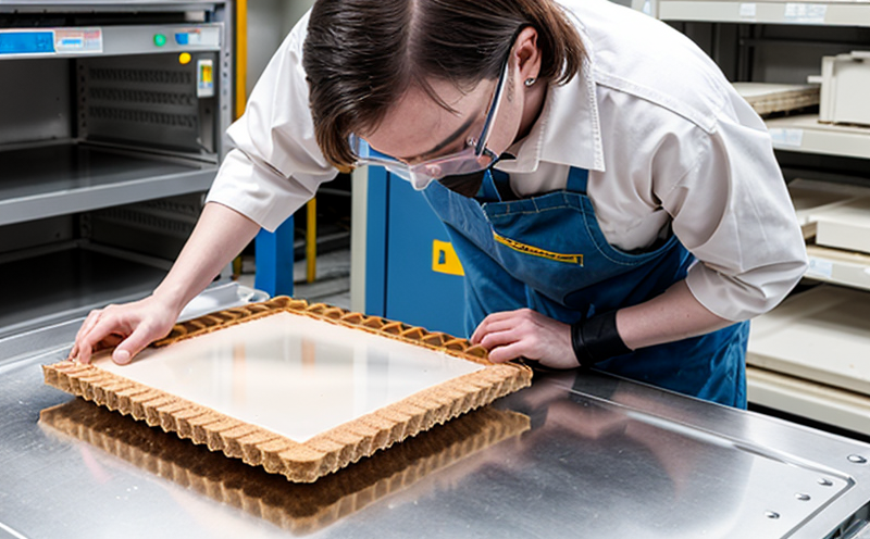
The testing process involves several critical steps: specimen preparation, calibration of equipment, and actual stress measurement. Specimen preparation includes selecting representative samples from production batches, cleaning them with appropriate solvents, and mounting them on a precision stage for measurement. Calibration ensures the accuracy of the test instruments, which are typically high-precision interferometric microscopes.
The actual testing process involves applying various mechanical loads to the wafer while monitoring changes in its optical properties using interferometry techniques. These tests provide detailed maps of internal stress distribution across different layers of the wafer. The results are analyzed according to SEMI M28 criteria, which define acceptable ranges for both normal and shear stresses.
Accurate measurement of these parameters is essential because even small deviations from standard can have a significant impact on device performance and reliability. For instance, excessive shear stress might lead to early failure in high-stress environments like automotive electronics or aerospace applications. Similarly, overly high normal stress could cause warping during the manufacturing process.
Compliance with SEMI M28 ensures that manufacturers deliver consistent product quality across batches. This consistency is crucial for maintaining customer trust and meeting regulatory requirements worldwide. Moreover, adherence to this standard helps reduce waste by identifying defective wafers early in the production cycle, thereby improving overall efficiency.
In summary, SEMI M28 wafer internal stress measurement testing plays a vital role in ensuring high-quality semiconductor manufacturing processes. It allows for precise control over critical parameters that influence device reliability and performance, ultimately contributing to better end-user experiences and more robust industrial applications.
Scope and Methodology
The scope of SEMI M28 wafer internal stress measurement testing encompasses the evaluation of both normal and shear stresses within silicon wafers. This includes measuring these stresses across various layers of the wafer, ensuring that they comply with specified limits set out by international standards such as ISO 45650:2018.
- Calibration of testing equipment to ensure accuracy.
- Preparation of representative specimens from production lots.
- Application of mechanical loads to simulate real-world conditions during processing or use.
- Monitoring changes in the wafer's optical properties through interferometry techniques.
- Analysis of stress distribution maps using specialized software tools.
The methodology adheres closely to SEMI M28 guidelines, which emphasize accurate and reproducible measurements. This ensures that all tests yield consistent results regardless of the laboratory or operator performing them.
Industry Applications
- Automotive Electronics: Ensures reliability in high-stress environments where even minor defects could lead to catastrophic failures.
- Aerospace: Critical for maintaining performance standards in mission-critical systems.
- Consumer Electronics: Enhances the longevity and durability of products used by consumers worldwide.
- Data Centers: Supports efficient operation by ensuring optimal cooling and power distribution.
Eurolab Advantages
At Eurolab, we pride ourselves on offering comprehensive SEMI M28 wafer internal stress measurement testing services tailored to meet the unique needs of our clients. Our state-of-the-art facilities and experienced team ensure that every test is conducted with precision and care.
- Accurate Results: Utilizing cutting-edge technology, we provide precise measurements that adhere strictly to SEMI M28 standards.
- Comprehensive Reporting: Detailed reports are generated for each test, providing insights into stress distribution and compliance with international norms.
- Expertise: Our staff comprises highly skilled professionals who stay updated on the latest developments in semiconductor testing techniques.


