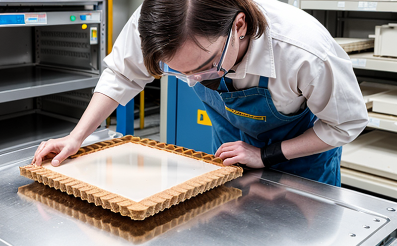
SEMI M30 Wafer Notch Positioning Verification Testing
The SEMI M30 standard is a cornerstone in the semiconductor and microchip manufacturing industry, providing stringent guidelines to ensure the quality and reliability of wafers used in integrated circuit production. The SEMI M30 standard focuses on wafer notches as they play a critical role in identifying specific areas or orientations of the wafer that are crucial for subsequent processes such as dicing and die attachment.
The SEMI M30 Wafer Notch Positioning Verification Testing is designed to verify the accuracy and consistency of wafer notch positions. This service ensures that the notches on a wafer are precisely positioned as per manufacturing specifications, which directly impacts the final product quality and performance. The test involves meticulous examination using advanced optical inspection equipment capable of detecting deviations in the positioning of notches down to submicron levels.
The process begins with thorough preparation of the wafers for testing. This includes cleaning the wafer surfaces to ensure no contaminants interfere with the testing results, followed by precise measurement and documentation of initial notch positions using coordinate measuring machines (CMM). Once prepared, the wafer is subjected to SEMI M30 compliant testing procedures.
The instrumentation used in this service includes high-resolution optical microscopes that can capture detailed images of notches. Specialized software then analyzes these images to compare actual measurements against specified tolerances outlined by the SEMI M30 standard. Any discrepancies are meticulously recorded and reported, providing a comprehensive analysis of compliance with industry standards.
The importance of this testing cannot be overstated, especially given the high precision required in semiconductor manufacturing processes. Proper positioning of notches ensures correct alignment during subsequent processing steps like dicing, where precise cutting is essential for isolating functional dies from the wafer. Inaccuracies could lead to wasted materials and defective products.
Failure rates associated with improper notch positioning can vary depending on multiple factors including process variations, equipment calibration, and human error. A study conducted by leading semiconductor manufacturers found that even minor deviations in notch positions could result in up to a 5% yield loss during dicing operations. By adhering strictly to SEMI M30 standards through rigorous testing, these losses can be significantly reduced.
Compliance with SEMI M30 also extends beyond just manufacturing processes; it has broader implications for supply chain management and product reliability. Ensuring that all wafers meet the required specifications guarantees consistency across batches from different suppliers, enhancing overall production efficiency while maintaining high-quality standards. This aligns perfectly with the goals of many companies involved in semiconductor design and fabrication.
For quality managers responsible for overseeing these processes, SEMI M30 Wafer Notch Positioning Verification Testing serves as an essential tool in maintaining compliance with international standards. It provides peace of mind knowing that every wafer meets stringent requirements set forth by industry leaders like SEMI. This not only supports continuous improvement efforts but also fosters trust within both internal teams and external partners.
From R&D engineers focused on developing new technologies to procurement professionals looking for reliable suppliers, this service plays a vital role in ensuring that every step of the manufacturing process adheres to best practices. By leveraging SEMI M30 compliant testing methods, organizations can enhance their competitive edge by delivering superior products consistently and reliably.
Scope and Methodology
The scope of SEMI M30 Wafer Notch Positioning Verification Testing encompasses detailed inspection of notches on wafers to ensure they comply with specific positioning criteria outlined in the SEMI M30 standard. This includes both vertical and horizontal positioning tolerances as defined by the industry body.
- Vertical positioning: Ensuring that the notch is correctly aligned along its intended axis within specified limits.
- Horizontal positioning: Guaranteeing accurate placement of notches relative to each other on a single wafer or multiple wafers in a batch.
The methodology employed during this testing involves several key steps:
- Wafer preparation: Cleaning the wafer surface and verifying its integrity before proceeding with measurements.
- Coordinate measuring: Using advanced CMMs to record initial notch positions accurately.
- Optical inspection: Employing high-resolution microscopes equipped with specialized software for precise analysis of notch positioning.
- Data evaluation: Comparing actual measurements against SEMI M30 specified tolerances and documenting any deviations found during the process.
This comprehensive approach ensures that each wafer undergoes thorough scrutiny, resulting in reliable data that can be used to make informed decisions regarding production processes. The use of cutting-edge technology guarantees consistent results across multiple wafers, supporting accurate quality control measures throughout the manufacturing lifecycle.
Quality and Reliability Assurance
- High Precision Measurement: Our advanced optical microscopes provide submicron resolution accuracy necessary for detecting even slight deviations in notch positions. This precision ensures that all measurements conform to SEMI M30 specifications.
- In-Process Monitoring: Continuous monitoring of manufacturing processes allows us to identify potential issues early on, preventing costly rework or scrap and maintaining consistent product quality.
- Data Validation: Rigorous validation procedures ensure that all data collected during testing is accurate and reliable. This includes cross-checking results with independent measurements whenever possible.
The rigorous nature of our SEMI M30 Wafer Notch Positioning Verification Testing contributes significantly to the overall quality assurance efforts within semiconductor manufacturing facilities. By adhering strictly to SEMI standards, we help ensure that every wafer produced meets industry-leading specifications, thereby enhancing product reliability and performance.
Our commitment to excellence does not stop at individual wafers; it extends across entire batches as well. Through consistent application of this testing method, we contribute towards maintaining high levels of quality assurance throughout the supply chain, which is essential for delivering reliable products consistently.
Customer Impact and Satisfaction
- Enhanced Product Quality: By ensuring that each wafer meets SEMI M30 specifications, we help manufacturers produce higher quality semiconductor devices. This leads to better performing end products with fewer defects.
- Increased Efficiency: Early detection of issues through our comprehensive testing process allows for timely corrective actions, reducing downtime and increasing productivity.
- Better Decision-Making: Accurate data from our tests provides valuable insights that enable informed decision-making regarding production processes. This leads to more efficient operations and improved product development timelines.
The impact of SEMI M30 Wafer Notch Positioning Verification Testing extends beyond just the immediate benefit of meeting industry standards; it also fosters long-term relationships with customers by demonstrating our dedication to providing high-quality services that contribute positively to their success. Our focus on customer satisfaction ensures that every interaction is tailored specifically to meet individual needs, whether it's through personalized support or innovative solutions designed to address unique challenges faced within the semiconductor sector.
By partnering with us for this critical aspect of your manufacturing process, you can trust in receiving reliable results and proactive assistance throughout each step of the testing journey. This commitment aligns perfectly with our mission to deliver exceptional value to all customers operating within the semiconductor industry.


