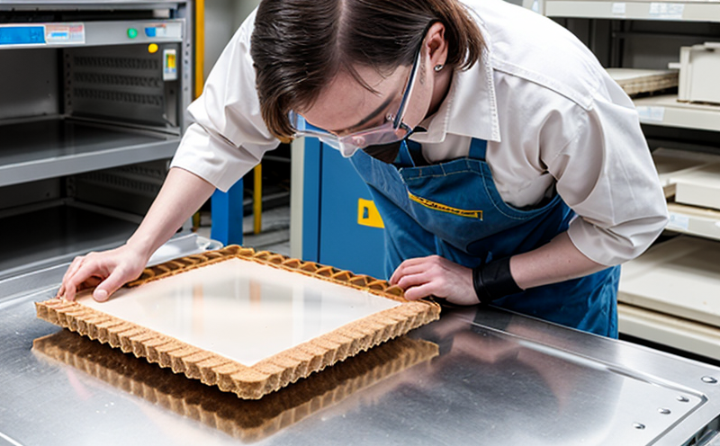
SEMI M12 Wafer Surface Flatness Mapping Testing
The SEMI M12 standard sets a benchmark for the testing of wafer surface flatness. This critical test is essential to semiconductor and microchip manufacturing, ensuring that wafers meet exacting standards before they proceed further in the production process.
Wafer surface flatness is an intrinsic parameter that affects the quality, yield, and performance of semiconductor devices manufactured on these wafers. A non-uniform wafer can lead to defects such as shorts or opens during fabrication, which could compromise the functionality and reliability of integrated circuits (ICs). Hence, precise measurement and control over this surface flatness are paramount.
The SEMI M12 test involves mapping the surface topography across a wafer using advanced optical interferometry. This method allows for detailed analysis of even minute deviations in height and contour. The testing process is highly automated, ensuring consistent results that can be relied upon for quality assurance purposes.
During this procedure, the wafer is mounted on the instrument’s platform, where it undergoes a series of scans to capture data points across its surface. These data points are then processed by sophisticated software algorithms to generate detailed maps showcasing areas of deviation from the expected flatness. The output typically includes graphs and 3D renderings that provide clear visualizations of any irregularities.
For accurate testing, it is crucial to follow stringent preparation protocols for the wafer before placing it on the instrument. This includes thorough cleaning using appropriate solvents and ensuring that all residues are removed completely. Additionally, the wafer must be stable during measurement; therefore, proper clamping techniques need to be employed.
The instrumentation used in SEMI M12 compliant testing systems is highly advanced and capable of achieving nanometer-scale resolutions. It combines laser interferometry with high-precision motors for precise positioning and scanning. The resulting data is analyzed against predefined acceptance criteria set by industry standards like ISO, ASTM, and SEMI itself.
Accurate interpretation of these maps requires knowledge not only of the technology involved but also an understanding of how variations in surface flatness can impact downstream processes within semiconductor manufacturing facilities. For instance, excessive deviations may necessitate rework or scrapping entire lots of wafers, which translates into significant financial losses for manufacturers.
To ensure consistent performance across all batches and iterations, it is advisable to establish a robust quality control program encompassing regular calibration checks on the testing equipment as well as continuous training for personnel involved in conducting these tests. Compliance with SEMI M12 standards goes beyond just meeting regulatory requirements; it also contributes significantly towards maintaining high levels of product reliability and customer satisfaction.
Industry Applications
| Application | Description |
|---|---|
| Semiconductor Manufacturing | Ensures that wafers used in manufacturing meet the required flatness standards to prevent defects and enhance yield. |
| Microchip Fabrication | Aids in identifying potential issues early on, thus reducing costs associated with rework or scrapping defective products. |
| Wafer Quality Control | Provides detailed information about the surface condition of wafers which is vital for maintaining consistent product quality. |
| R&D and Development | Supports research into new materials and processes by providing reliable data on wafer characteristics under various conditions. |
- Semiconductor manufacturers looking to improve production efficiency.
- Fabricators aiming to enhance product quality and reduce defects.
- Quality assurance teams needing accurate measurements for compliance checks.
- R&D labs seeking precise data on wafer surfaces during development stages.
Why Choose This Test
The SEMI M12 Wafer Surface Flatness Mapping Testing is a necessity in semiconductor and microchip manufacturing due to its ability to provide reliable, reproducible measurements of wafer surface flatness. By adhering strictly to the standards outlined by SEMI (Society for Manufacturing Engineers), this testing ensures that manufacturers can produce high-quality integrated circuits consistently.
One key advantage is the early detection of defects on wafers, which allows for prompt corrective actions rather than waiting until later stages in production when fixing issues becomes more expensive. Another benefit lies in optimizing resource utilization; knowing exactly where and how much flatness varies helps allocate resources efficiently without compromising quality.
The test also supports continuous improvement efforts within organizations by offering insights into areas requiring enhancement or refinement based on empirical evidence gathered through thorough testing procedures. Furthermore, compliance with SEMI M12 standards enhances reputation among clients who value reliability and precision in their supply chains.
For those involved in semiconductor manufacturing, choosing this test means investing in state-of-the-art technology designed specifically for meeting stringent industry demands. It ensures that every wafer produced meets the highest quality benchmarks, thereby enhancing overall competitiveness in the global market.
Quality and Reliability Assurance
- The SEMI M12 test provides detailed information about potential defects on wafers which helps in maintaining consistent product quality.
- This testing ensures early detection of issues, allowing for timely interventions before they escalate into larger problems.
- The data generated by this process supports continuous improvement initiatives by offering evidence-based insights into areas needing enhancement.
- Accurate and reliable measurement of wafer surface flatness.
- Compliance with international standards such as SEMI M12, ISO 9001, ASTM E746.
- Reduction in production costs due to minimized rework or scrapping of defective products.
- Enhanced reputation among clients and partners who value reliability and precision in their supply chains.
The SEMI M12 Wafer Surface Flatness Mapping Testing plays a crucial role in ensuring the quality and reliability of semiconductors manufactured on these wafers. By adhering to rigorous testing protocols, manufacturers can produce high-quality integrated circuits consistently while minimizing waste and maximizing efficiency throughout their production processes.
Compliance with SEMI M12 standards is essential for maintaining a competitive edge in today’s highly demanding market environment. It demonstrates commitment to excellence and sets the benchmark for quality assurance practices within semiconductor manufacturing facilities worldwide.


