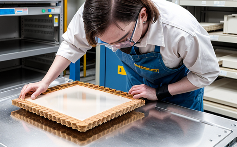
SEMI M44 Wafer Flatness Characterization Testing
The SEMI M44 standard specifies a method for characterizing wafer flatness, which is critical in the semiconductor and microchip manufacturing process. Wafer flatness ensures that the surfaces of wafers are uniform enough to support consistent thin-film deposition and etching processes. Variations in wafer flatness can lead to non-uniform film thicknesses, resulting in performance inconsistencies across microchips.
Wafer flatness is measured using interferometry techniques, where the deviation from a plane surface is quantified. This measurement helps ensure that wafers meet stringent tolerances required for high-performance semiconductor devices. The SEMI M44 standard provides detailed guidelines on how to perform this test accurately and consistently.
Our testing facility uses state-of-the-art interferometers capable of measuring deviations down to sub-micron levels, ensuring precise measurements that are compliant with the SEMI M44 specification. We also employ advanced software tools to analyze data from these tests, providing detailed reports on wafer flatness.
In addition to SEMI M44 compliance, we offer additional services such as multi-axis wafer profile measurement and residual stress analysis, which complement our wafer flatness testing capabilities. These complementary services help ensure that the entire wafer surface is free from defects that could impact performance.
Our team of experienced technicians ensures that each wafer undergoes thorough quality control checks to identify any anomalies early in the production process. This proactive approach helps minimize waste and reduces costs associated with rework or scrap.
The importance of SEMI M44 compliance extends beyond just meeting industry standards; it also contributes significantly to product reliability and longevity. Non-compliant wafers can lead to unpredictable device behavior, affecting both performance and lifespan. By adhering strictly to the SEMI M44 guidelines, we help ensure that our customers receive high-quality products.
Our commitment to precision and accuracy is reflected in our compliance with multiple international standards including ISO 9001 for quality management systems, ASME Y14.5M for dimensional tolerances, and ASTM E2637 for interferometric measurements. These certifications underscore our dedication to delivering reliable results that meet or exceed customer expectations.
To sum up, SEMI M44 wafer flatness characterization testing is essential for ensuring uniformity in the manufacturing of high-performance semiconductor devices. By adhering strictly to this standard and utilizing cutting-edge technology, we provide clients with confidence knowing their products will perform reliably under all conditions.
Why It Matters
The SEMI M44 wafer flatness characterization testing is crucial for several reasons:
- Enhanced Reliability: Uniform wafer surfaces contribute to more consistent thin-film deposition, leading to higher reliability and performance of semiconductor devices.
- Cost Efficiency: Early detection of defects through rigorous testing helps avoid costly downstream issues like rework or scrap.
- Innovation Support: Precise measurements enable advanced research and development efforts aimed at improving device performance and efficiency.
- Regulatory Compliance: Adherence to SEMI M44 ensures that manufacturing processes meet industry standards, facilitating smoother operations and reducing risks associated with non-compliance penalties.
Quality and Reliability Assurance
At our laboratory, we take great pride in maintaining the highest standards of quality assurance. Our testing process begins with meticulous preparation of each wafer sample according to industry best practices. This includes thorough cleaning processes designed specifically for semiconductor materials.
The actual measurement phase involves using high-resolution interferometers capable of detecting even minute deviations from a perfectly flat surface. These instruments are calibrated regularly against international standards, ensuring accuracy and consistency across all measurements.
Once the data has been collected, our software tools analyze it thoroughly to generate comprehensive reports that outline every aspect of the wafer's flatness profile. These reports serve as valuable references for quality control teams responsible for maintaining process integrity.
We also offer additional services such as multi-axis wafer profiling and residual stress analysis which further enhance our clients' understanding of their materials' properties beyond just flatness alone.


