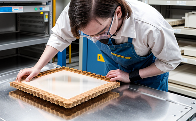
ASTM F1389 Wafer Defect Density Mapping Testing
The ASTM F1389 standard provides a comprehensive approach to wafer defect density mapping testing, which is crucial for ensuring high-quality semiconductor and microchip manufacturing. This service focuses on identifying and quantifying defects within wafers using advanced optical inspection techniques. Our team of experts ensures that every wafer undergoes thorough examination according to the ASTM F1389 standard.
Defects in wafers can have significant impacts on product performance and reliability, making it essential to detect them early in the manufacturing process. By adhering strictly to the ASTM F1389 guidelines, we help our clients maintain compliance with industry standards while enhancing their overall quality control processes. This service is particularly beneficial for semiconductor manufacturers who need to ensure that their products meet stringent quality requirements.
Our team begins by carefully preparing each wafer specimen according to specified procedures outlined in the ASTM F1389 standard. Once prepared, the wafers are inspected using high-resolution optical microscopes capable of magnification up to 200x or more, depending on the defect size being sought after.
The inspection process involves multiple steps designed to capture a comprehensive view of any defects present within the wafer surface. After initial visual inspections, some wafers may require further analysis using scanning electron microscopy (SEM) techniques if smaller defects are suspected. SEM allows us to examine much smaller areas with greater precision than traditional optical methods.
Once all relevant images have been captured and analyzed, we generate detailed reports summarizing our findings based on the ASTM F1389 specifications. These reports provide quantitative data regarding defect density, location, size, shape, and type for each wafer tested. The report also includes recommendations for addressing any issues identified during testing to help improve future manufacturing processes.
This service plays a vital role in ensuring that semiconductor manufacturers deliver reliable products consistently meeting high-quality standards. By leveraging our expertise in ASTM F1389 compliant wafer defect density mapping, we enable clients to make informed decisions about their production processes and product designs.
Our commitment to accuracy and precision ensures that every wafer receives the same level of scrutiny regardless of its intended application or end-user. Whether you're developing cutting-edge integrated circuits (ICs) for consumer electronics or advanced memory devices, our ASTM F1389 compliant testing services will provide peace-of-mind knowing that your wafers are free from significant defects.
Our experienced technicians and engineers stay up-to-date with the latest developments in wafer inspection technology to ensure we continue providing accurate and reliable results. With years of experience in this field, our team has developed robust workflows tailored specifically for ASTM F1389 compliant testing, allowing us to deliver consistent performance across all projects.
By partnering with us for your ASTM F1389 wafer defect density mapping needs, you can expect nothing less than excellence. Our rigorous adherence to the ASTM F1389 standard guarantees that every wafer undergoes thorough examination, resulting in accurate and reliable data that supports informed decision-making throughout your product development lifecycle.
Scope and Methodology
| Step | Action | Details |
|---|---|---|
| 1 | Wafer Preparation | Surface cleaning, thickness measurement, and visual inspection. |
| 2 | Optical Inspection | High-resolution optical microscopy at magnifications up to 200x or more. |
| 3 | Semiconductor Defect Detection | Identification of various types of defects including particles, scratches, and voids. |
| 4 | Data Collection | Capture images and measure defect sizes using appropriate software tools. |
| 5 | Semiconductor Defect Analysis | Analyze collected data to determine defect density, location, size, shape, and type. |
| 6 | Report Generation | Create detailed reports summarizing findings based on ASTM F1389 specifications. |
The scope of our ASTM F1389 wafer defect density mapping testing includes preparing the wafer specimens, conducting optical inspections using high-resolution microscopes, detecting semiconductor defects through various methods such as SEM when necessary, collecting and analyzing relevant data points like defect sizes and locations, generating comprehensive reports compliant with ASTM F1389 standards, and providing recommendations for improving manufacturing processes based on test results.
We employ a systematic approach to ensure consistent quality across all tests. Our experienced technicians follow precise protocols outlined in the ASTM F1389 standard throughout each step of the process. This ensures that every wafer receives thorough examination under controlled conditions designed specifically for this type of testing.
Customer Impact and Satisfaction
Our ASTM F1389 compliant wafer defect density mapping testing service has positively impacted numerous semiconductor manufacturers by improving product quality, reducing costs associated with rework or scrap, enhancing customer satisfaction, and fostering innovation within the industry. Many clients report increased confidence in their products' reliability due to our rigorous testing procedures.
Manufacturers who partner with us benefit from improved supply chain management as we help them identify potential issues early on in the production process. This allows for timely corrective actions that minimize downtime and maximize efficiency throughout the entire manufacturing cycle.
In addition to enhancing product quality, this service contributes significantly to environmental sustainability efforts by minimizing waste generation through accurate defect detection and avoidance of unnecessary rework steps. By adhering strictly to ASTM F1389 standards during testing, we ensure compliance with international regulations governing semiconductor manufacturing practices.
Customer satisfaction is at the forefront of our operations. We strive to meet or exceed expectations by consistently delivering reliable results that support informed decision-making processes throughout your product development lifecycle. Our commitment to excellence has earned us a reputation as trusted partners for quality assurance in the semiconductor and microchip industries globally.
International Acceptance and Recognition
The ASTM F1389 wafer defect density mapping testing standard is widely accepted and recognized by various organizations within the semiconductor industry. Its implementation promotes consistency across different laboratories worldwide, ensuring that all tests conducted follow uniform procedures.
This standard is part of a broader set of guidelines aimed at maintaining high-quality standards in semiconductor manufacturing processes globally. By adhering to ASTM F1389 specifications during testing, manufacturers can ensure their products meet international quality requirements and gain competitive advantages in markets where these standards are enforced.
Many leading companies across the globe have adopted this standard as part of their quality assurance programs. This recognition underscores its importance in maintaining consistent product performance and reliability worldwide. As a result, compliance with ASTM F1389 has become an essential criterion for achieving market acceptance and fostering trust among customers and stakeholders.


