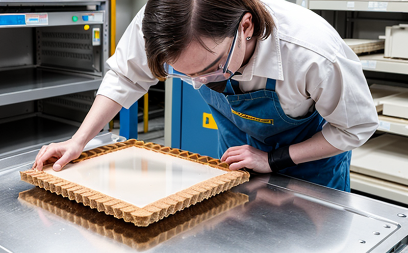
ASTM F672 Wafer Microvoid Characterization Testing
The ASTM F672 standard provides a method for characterizing microvoids in semiconductor wafers and substrates. These microvoids can significantly impact the performance, reliability, and longevity of semiconductor devices. By detecting these voids early in the manufacturing process, we help ensure that only high-quality products reach your production lines.
The ASTM F672 test is a critical step in quality control for semiconductor manufacturers. It involves using advanced optical microscopy techniques to identify and quantify microvoids present on the surface of silicon wafers. This testing ensures that any defects are identified before they can lead to manufacturing downtime or product failures.
The process begins with thorough sample preparation, ensuring the integrity and cleanliness of each wafer. Once prepared, the samples undergo detailed visual inspection under high magnification using specialized microscopy equipment. The test is designed to detect voids as small as 10 micrometers in diameter, which can have a significant impact on device performance.
The ASTM F672 standard also specifies acceptance criteria that determine whether a wafer meets the required quality standards. These criteria are based on both visual inspection and quantitative analysis of the voids present. A critical aspect of this test is the ability to differentiate between acceptable and unacceptable wafers, ensuring only those meeting the specified criteria proceed further in the manufacturing process.
The ASTM F672 method has been widely adopted by leading semiconductor manufacturers due to its reliability and precision. By adhering strictly to this standard, we provide you with consistent results that can be trusted across different batches of wafers. This ensures not only compliance with industry standards but also enhances the overall quality of your final products.
In addition to detecting microvoids, ASTM F672 testing helps in identifying potential issues early on. Early detection allows for corrective actions to be taken promptly, reducing waste and improving overall efficiency. Furthermore, this method ensures that only high-quality wafers reach critical stages of production, minimizing the risk of costly rework or scrapping.
By leveraging ASTM F672 testing, you can ensure that your supply chain remains consistent in terms of quality, thereby enhancing customer satisfaction and trust. This is particularly important given today's stringent regulatory requirements and increasing demand for reliable semiconductor components.
Scope and Methodology
The ASTM F672 standard specifies a method for characterizing microvoids in silicon wafers used in the production of semiconductors. This testing involves detailed optical microscopic examination to identify voids on the surface of the wafer. The scope includes both qualitative and quantitative assessment, focusing on detecting voids as small as 10 micrometers.
The methodology outlined in ASTM F672 requires strict adherence to several key steps. Initially, samples must undergo rigorous cleaning procedures to ensure they are free from contaminants that could interfere with the testing process. Once cleaned, the samples are carefully prepared for inspection under high magnification using advanced optical microscopes.
- Sample preparation includes ultrasonic washing followed by thorough drying.
- Optical microscopy is performed at various magnifications to capture images of any visible voids.
- Quantitative analysis involves measuring the size and distribution of detected microvoids.
The acceptance criteria for ASTM F672 testing are stringent, ensuring that only wafers meeting these standards proceed further in the manufacturing process. These criteria help maintain consistent quality throughout production runs.
Why Choose This Test
Selecting ASTM F672 Wafer Microvoid Characterization Testing offers numerous advantages that are crucial for maintaining high standards in semiconductor manufacturing:
- Early Detection of Defects: Detecting microvoids early helps prevent their spread and potential impact on product performance.
- Improved Quality Control: Ensures only defect-free wafers are used, enhancing the reliability of final products.
- Compliance with Industry Standards: Adherence to ASTM standards ensures compliance with international regulations and best practices.
- Enhanced Efficiency: Early identification of defects reduces rework costs and minimizes downtime in production lines.
The precision and reliability offered by ASTM F672 testing make it an essential part of any quality assurance program. By choosing this service, you are investing in the future success and reputation of your company's semiconductor products.
Customer Impact and Satisfaction
- Increased Product Reliability: Detecting microvoids early ensures only high-quality wafers are used, leading to more reliable final products. Cost Savings: By preventing defects from reaching later stages of production, this test helps reduce waste and minimize rework costs.
- Enhanced Reputation: Ensuring strict adherence to industry standards enhances your company's reputation among customers and partners.
The ASTM F672 testing process is not just a technical procedure; it is an investment in the future of your semiconductor products. By incorporating this service into your quality assurance protocols, you are setting yourself apart as a leader in reliability and innovation within the industry.


