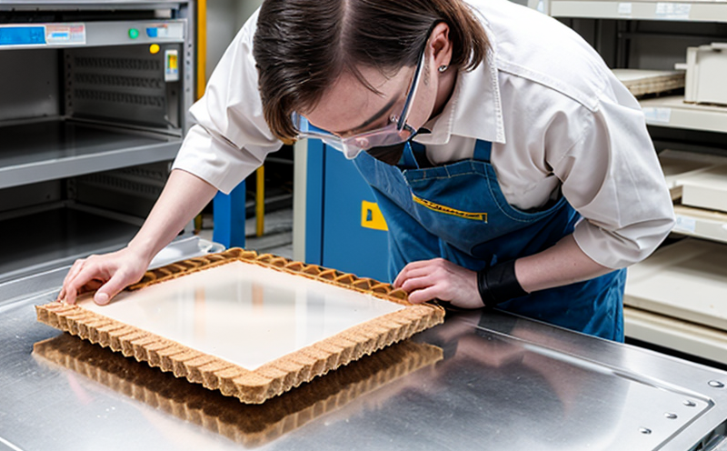
ASTM F1351 Wafer Edge Strength Testing
The ASTM F1351 standard specifies a method for determining the edge strength of semiconductor wafers, which is critical for ensuring the integrity and reliability of microchips. This test evaluates how well the edges can withstand mechanical stress without failing, thus preventing potential defects that could impact the performance or lifespan of integrated circuits.
The testing process involves subjecting a specimen to controlled shear forces until it breaks at its weakest point along the edge. The force required for failure is then measured and recorded as an indicator of the wafer’s edge strength. This information is vital not only for quality assurance but also in optimizing manufacturing processes, ensuring consistent product performance across batches.
For semiconductor manufacturers, ASTM F1351 testing helps identify weak points in the manufacturing process that could lead to failures during production or use. By understanding these weaknesses early on, companies can implement corrective measures to improve yield rates and reduce costly rework or scrap. Additionally, this test supports compliance with industry standards, enhancing credibility among customers who rely on high-quality semiconductor products.
The ASTM F1351 procedure is particularly important when dealing with large diameter wafers used in cutting-edge technologies like 45nm or smaller nodes. These advanced materials often have more complex structures and thinner layers compared to traditional silicon substrates, making them even more susceptible to edge damage during handling and processing.
Manufacturers must ensure that their testing facilities meet all requirements outlined by ASTM F1351 to guarantee accurate results. Properly trained personnel using appropriate equipment are essential for obtaining reliable data from this type of test. Compliance with these standards ensures consistent quality across all batches produced, which is crucial given the increasingly competitive nature of the semiconductor industry.
| Standard | Description |
|---|---|
| ASTM F1351-20 | Determination of edge strength of semiconductor wafers. |
Why It Matters
The integrity and reliability of semiconductor products depend heavily on the quality of their constituent materials. Edge strength testing is one way to assess this critical aspect, ensuring that wafers are robust enough to withstand various stresses encountered throughout fabrication processes and subsequent assembly steps.
- Prevents defects caused by mechanical failures due to edge weaknesses.
- Ensures compliance with industry standards set forth by organizations such as ASTM.
- Supports continuous improvement efforts aimed at enhancing overall product performance.
- Aids in identifying areas where process optimizations can be made, thereby increasing efficiency and reducing costs associated with rework or scrap.
Applied Standards
The ASTM F1351-20 standard provides detailed procedures for conducting edge strength tests on semiconductor wafers. It covers all aspects from selecting appropriate specimens to analyzing the resulting data, ensuring that laboratories performing these tests follow consistent methodologies.
Quality and Reliability Assurance
- Regular calibration of testing equipment to maintain precision and accuracy.
- Training of personnel on proper techniques for specimen preparation and handling.


