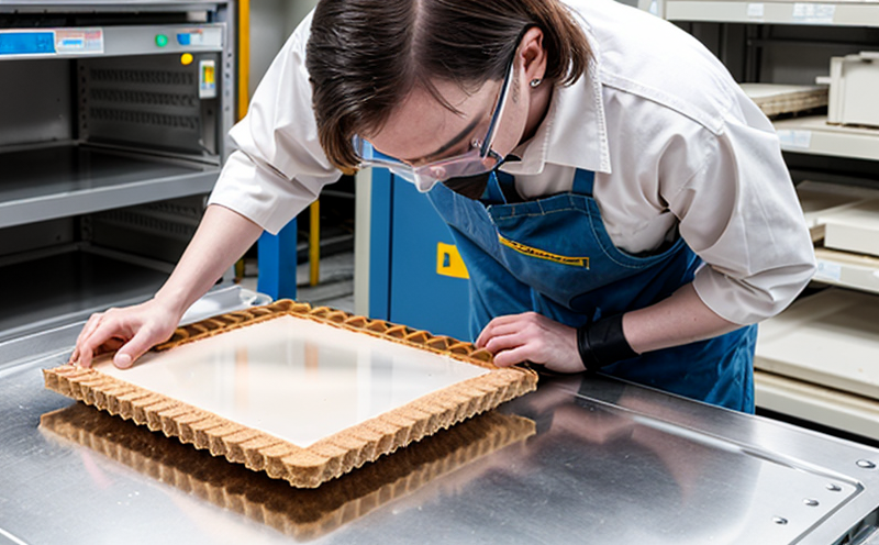
ASTM F736 Wafer Planarity Measurement Testing
The ASTM F736 standard specifies a method for determining wafer planarity, which is crucial in the semiconductor and microchip manufacturing processes. Wafer planarity refers to how flat or uniform a silicon wafer’s surface is after processing. Variations in planarity can lead to inconsistencies in chip performance, yield losses, and even product failures.
The testing process involves measuring the height of the wafer at various points using optical profilometry techniques. The goal is to ensure that any deviations from a perfectly flat surface are within acceptable limits defined by the standard. This ensures that wafers meet the stringent requirements needed for high-quality semiconductor manufacturing.
Accurate planarity measurement is critical because even minute irregularities can affect how photolithography, etching, and other processes interact with the wafer’s surface. The testing procedure outlined in ASTM F736 ensures that wafers are consistent across all areas, which is essential for producing reliable microchips.
The measurement process typically involves the use of a profilometer, which scans the wafer’s surface to create a topographical map. This map is then analyzed to determine the maximum and minimum deviations from an ideal plane. The results are compared against the tolerances specified in ASTM F736 to ensure compliance.
The importance of this testing cannot be overstated, especially given the high precision required in semiconductor manufacturing. Even minor irregularities can lead to significant issues during subsequent stages of chip production. By adhering strictly to ASTM F736, manufacturers can minimize these risks and produce higher quality wafers.
The standard defines specific tolerances for different wafer sizes, which are critical for ensuring that the testing process is consistent across various types of wafers used in the industry. Understanding these requirements helps ensure that all test results are comparable and meaningful.
In summary, ASTM F736 Wafer Planarity Measurement Testing plays a vital role in semiconductor manufacturing by providing a standardized method for assessing wafer flatness. This ensures that manufacturers can produce consistent, high-quality wafers that meet the stringent requirements of modern microchip design.
Benefits
The ASTM F736 Wafer Planarity Measurement Testing offers several significant benefits to semiconductor and microchip manufacturers:
Quality Control: By ensuring that wafers meet the specified planarity standards, this testing method helps maintain consistent product quality. This reduces the likelihood of defects during manufacturing processes.
Cost Efficiency: Early detection of non-compliant wafers through rigorous testing can prevent costly rework and scrapped materials.
Compliance: Adhering to industry standards like ASTM F736 ensures that manufacturers meet regulatory requirements, which is essential for maintaining a strong market reputation.
Product Reliability: Consistent planarity leads to more reliable microchips, enhancing overall product performance and longevity.
Innovation Support: High-quality wafers are crucial for advancing semiconductor technology. ASTM F736 supports continuous improvements in manufacturing processes.
Quality and Reliability Assurance
The ASTM F736 Wafer Planarity Measurement Testing is integral to the quality assurance process in semiconductor manufacturing. Ensuring that wafers are within the specified tolerances helps prevent defects that could lead to product failures or performance issues.
By implementing this testing method, manufacturers can establish a robust quality control system that enhances overall reliability and reduces production errors. This not only improves the efficiency of the manufacturing process but also contributes to the development of more advanced semiconductor technologies.
The stringent tolerances defined in ASTM F736 ensure that each wafer undergoes thorough evaluation, which is critical for maintaining the highest standards of quality. This approach helps manufacturers stay ahead of industry trends and meet the growing demand for high-performance microchips.
Use Cases and Application Examples
The ASTM F736 Wafer Planarity Measurement Testing is widely used in various semiconductor manufacturing processes. Here are some key use cases:
Photolithography: Ensuring that the wafer surface is flat minimizes misalignment issues during photolithography, which is essential for accurate pattern transfer.
Etching Processes: Consistent planarity prevents etching errors that could lead to uneven feature depths and poor uniformity.
Cleaning Procedures: Flat surfaces are easier to clean uniformly, ensuring that all areas of the wafer receive consistent treatment.
Patterning Precision: The precision required in patterning is significantly improved by flat wafers, which enhances overall manufacturing accuracy.
Doping Consistency: Flat surfaces ensure uniform doping distribution, leading to more reliable and efficient semiconductor devices.
Thermal Cycling: Consistent planarity helps in achieving uniform thermal cycling behavior, which is crucial for the durability of microchips.


