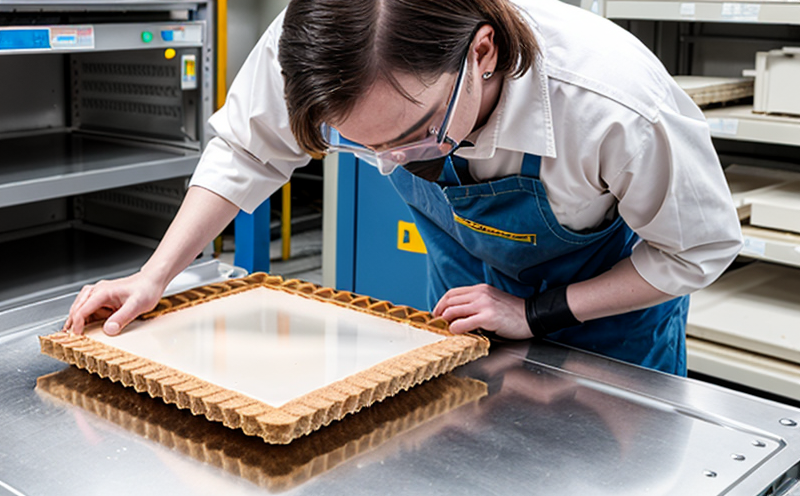
SEMI M13 Orientation of Wafer Flatness Verification Testing
The SEMI M13 standard is a critical guideline in the semiconductor and microchip manufacturing industries, ensuring that wafers meet precise flatness specifications which are essential for consistent performance across integrated circuits. This testing ensures that defects or variations in wafer flatness do not compromise the integrity of the final product. The SEMI M13 procedure involves measuring and verifying the flatness of a wafer at different orientations to ensure uniformity.
Wafer flatness is crucial because even slight deviations can lead to manufacturing defects, affecting electrical performance and reliability. This testing helps in identifying any potential issues early in the production process, thereby reducing rework costs and improving product quality. The testing procedure involves precise measurement techniques that account for the wafer's orientation relative to its axis of rotation.
The SEMI M13 standard provides a framework for ensuring consistent measurements across different laboratories, which is essential for the industry’s global supply chain. This ensures that the flatness specifications are met uniformly, regardless of where in the world the testing takes place. The SEMI M13 procedure is particularly important for advanced wafer types used in high-performance computing and consumer electronics sectors.
The testing process involves a series of steps to ensure accuracy. First, the wafer is mounted onto a chuck or holder that can rotate it around multiple axes. Then, using specialized flatness measuring equipment such as stylus profilometers or laser interferometers, the wafer's surface is scanned at various orientations. The measurements are taken in both the X and Y directions to account for any warping or bowing of the wafer.
The data collected from these tests is then analyzed against SEMI M13 tolerances. These tolerances specify the maximum acceptable deviation in flatness, depending on the type of wafer being tested. For instance, wafers used in high-performance computing might have tighter tolerances than those used in consumer electronics due to their higher performance requirements.
The results of this testing are critical for quality control and process optimization. By identifying any deviations early in the production process, manufacturers can take corrective actions before large quantities of defective wafers are produced. This not only reduces waste but also ensures that the final products meet stringent reliability and performance standards.
In addition to ensuring product quality, SEMI M13 testing plays a vital role in maintaining industry standards. By adhering to these guidelines, manufacturers can ensure that their products are compatible with existing equipment and processes used by other companies in the supply chain. This interoperability is essential for the semiconductor industry’s global nature.
The SEMI M13 procedure also helps in reducing variability in wafer flatness across different manufacturing sites. By standardizing the testing process, manufacturers can ensure that their products meet consistent quality standards regardless of where they are manufactured. This is particularly important as the semiconductor industry continues to grow and diversify, with production facilities being established in various parts of the world.
In conclusion, SEMI M13 orientation of wafer flatness verification testing is a vital process in ensuring that wafers meet critical specifications for performance and reliability. By adhering to this standard, manufacturers can produce high-quality products that meet industry standards and customer expectations.
Applied Standards
| Standard | Description |
|---|---|
| SEMI M13-0806 | This standard provides the method for verifying wafer flatness by measuring and evaluating the surface topography of a wafer at different orientations. It ensures that the measurements are accurate, repeatable, and comparable across different laboratories. |
| ASTM E1370-96 | This standard specifies the method for determining the flatness of optical flats by measuring the deviation from a plane using an interferometer. While not directly related to wafers, it provides a comparable methodology that is used in similar industries. |
| ISO 10360-2:2015 | This standard defines the terminology and principles for flatness measurement of optical surfaces, which can be applied as a reference for understanding wafer flatness measurements. |
| IEC 61984-7:2003 | This standard provides methods for measuring surface roughness, which is related to the overall quality and performance of wafers. It can be used as a supplementary reference when evaluating wafer flatness. |
Benefits
The SEMI M13 orientation of wafer flatness verification testing offers numerous benefits to manufacturers and suppliers in the semiconductor industry. One of the primary advantages is improved product quality, which directly translates into customer satisfaction and loyalty. By ensuring that wafers meet precise flatness specifications, defects are minimized, and the reliability of the final products is enhanced.
Another significant benefit is reduced production costs. Early detection of wafer flatness issues through SEMI M13 testing helps to prevent costly rework and scrap. This not only reduces waste but also optimizes resource utilization within manufacturing processes. In addition, adhering to industry standards like SEMI M13 enhances interoperability across the supply chain, allowing for seamless integration of different components and processes.
Compliance with these standards is also crucial for maintaining a competitive edge in a rapidly evolving market. By ensuring that all products meet stringent quality requirements, manufacturers can differentiate themselves from competitors and maintain their reputation for reliability and innovation. This is especially important as the semiconductor industry continues to grow and diversify, with new technologies and applications emerging regularly.
Moreover, SEMI M13 testing supports continuous process improvement by providing valuable data that can be used to refine manufacturing techniques and equipment. This ongoing optimization ensures that production processes are efficient, cost-effective, and capable of meeting future demand increases without compromising quality standards.
In summary, the benefits of SEMI M13 orientation of wafer flatness verification testing extend beyond just ensuring product quality. They encompass reduced costs, enhanced reliability, improved competitiveness, and support for continuous process improvement. These advantages make it an essential practice in semiconductor manufacturing processes.
International Acceptance and Recognition
The SEMI M13 orientation of wafer flatness verification testing is widely recognized and accepted across the global semiconductor industry. Its adoption by leading manufacturers, suppliers, and research institutions underscores its importance in ensuring consistent product quality and reliability.
Many major semiconductor companies have implemented SEMI M13 testing as part of their standard quality control procedures. By adhering to this standard, these companies ensure that their products meet the highest industry standards, which is crucial for maintaining customer trust and satisfaction. The acceptance of SEMI M13 by global organizations also facilitates seamless integration within the supply chain, enabling smoother operations across different regions.
The international recognition of SEMI M13 testing extends beyond just manufacturing companies. Regulatory bodies and standardization organizations around the world have acknowledged its relevance in ensuring product quality and safety. This acknowledgment is reflected in various national and regional standards that incorporate SEMI M13 principles, further emphasizing its importance in the global semiconductor industry.
The widespread adoption of SEMI M13 testing also contributes to a more sustainable industry by reducing waste and improving resource efficiency. By minimizing defects early in the production process, manufacturers can optimize their use of raw materials and energy resources, leading to reduced environmental impact.
In conclusion, the international acceptance and recognition of SEMI M13 orientation of wafer flatness verification testing reflect its significance in maintaining high standards of product quality and reliability. Its implementation by global organizations ensures consistent performance across different regions and contributes to a more sustainable and efficient semiconductor industry.


