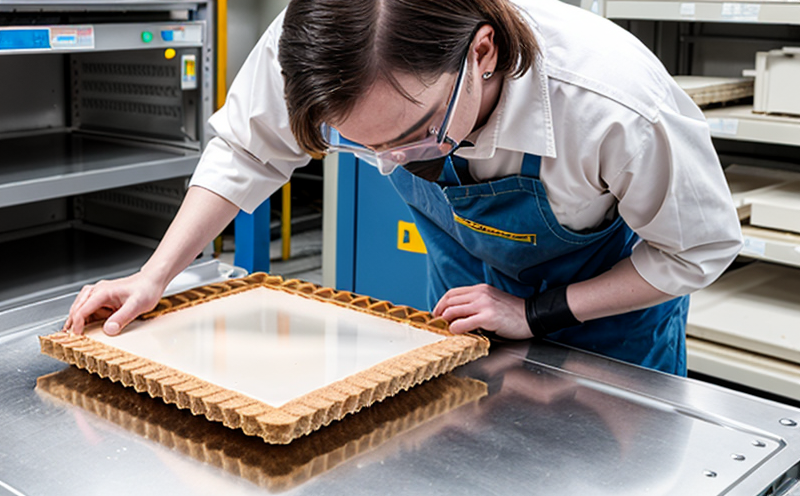
SEMI M35 Wafer Stress Mapping Testing
The SEMI M35 standard is a critical guideline in the semiconductor industry for wafer stress mapping. This testing ensures that wafers are free from excessive mechanical stresses, which can lead to defects and failures during manufacturing processes or subsequent use.
Stress within a silicon wafer can be caused by various factors such as thermal expansion, chemical etching, and mechanical deformation. These stresses can have significant implications on the performance of microchips, potentially leading to electrical shorts or open circuits. SEMI M35 testing provides a methodical approach to identify and quantify these stresses.
The test involves precise measurement techniques that can detect stress levels down to the nanometer scale. The process typically starts with careful preparation of the wafer surface to ensure accurate readings. This includes cleaning, degreasing, and sometimes applying a thin film to protect the wafer during testing.
Once prepared, the wafer is subjected to various mechanical or thermal treatments that simulate real-world conditions it might encounter in production or use. The stress measurement devices used for this purpose are highly sensitive and capable of capturing even minute changes in stress distribution across the wafer's surface.
The SEMI M35 standard specifies detailed procedures for testing, including sample preparation, equipment calibration, and data analysis. Compliance with these standards is essential to ensure consistency and reliability in semiconductor manufacturing processes. Failure to meet these standards can result in non-conforming products that may not function as intended or could fail prematurely.
Accurate stress mapping is crucial for quality control, especially in high-performance applications like advanced CPUs and GPUs where even small variations in stress distribution can affect performance and reliability. By adhering to the SEMI M35 standard, manufacturers can produce wafers that meet stringent quality standards and ensure their products are reliable and durable.
Quality managers and R&D engineers rely on these tests to optimize production processes and improve product design. Compliance officers also play a vital role in ensuring that all testing adheres to international standards like SEMI M35, thereby maintaining the integrity of the supply chain.
The SEMI M35 standard is widely recognized for its rigorous approach to wafer stress mapping, making it an indispensable tool in the semiconductor industry. By using this method, manufacturers can produce high-quality wafers that meet the demands of both current and future technologies.
Industry Applications
The SEMI M35 standard finds extensive application across various segments of the semiconductor industry. It is particularly critical in the wafer fabrication process, where stress mapping helps identify potential issues early on and ensures that wafers meet stringent quality standards.
- Wafer Fabrication: Early detection of stress-related defects through SEMI M35 testing can prevent costly rework or scrapped materials. This results in significant savings for manufacturers by optimizing production yields.
- Advanced Manufacturing Processes: In the era of increasingly complex microchips, stress mapping is essential to maintain consistent quality across large-scale productions. It ensures that even the most advanced fabrication techniques do not introduce unacceptable levels of stress into the wafers.
- R&D and Design Optimization: By providing detailed stress maps, SEMI M35 testing aids in refining design processes. Engineers can use this information to make informed decisions about material selection and process parameters that minimize stress generation.
The standard is also valuable for quality assurance departments, helping them maintain product consistency and reliability. Compliance with the SEMI M35 standard is a key factor in ensuring that semiconductor products meet industry benchmarks and customer expectations.
Why Choose This Test
Selecting SEMI M35 wafer stress mapping testing offers several advantages over other methods. Firstly, it provides precise and reliable data on the distribution of stresses within wafers. This precision is crucial for identifying subtle variations that could otherwise go unnoticed with less accurate techniques.
Secondly, this method allows manufacturers to implement proactive quality control measures. By detecting stress-related issues early in the production process, companies can address them before they escalate into larger problems, thereby improving overall product reliability and performance.
Another significant advantage is the ability to customize testing protocols to suit specific requirements. This flexibility ensures that the tests are relevant to each manufacturer's unique processes and end-product specifications. It also supports continuous improvement efforts by providing actionable insights from stress mapping data.
The SEMI M35 standard is supported by a robust network of laboratories equipped with state-of-the-art equipment. These facilities ensure consistent testing conditions, which translates into more accurate and repeatable results. This consistency builds trust among clients and stakeholders, reinforcing the reliability of the testing process.
Moreover, compliance with SEMI M35 standards enhances reputation within the industry. It demonstrates a commitment to quality and adherence to best practices, which can lead to increased market confidence and better business relationships. In an increasingly competitive landscape, such credibility is invaluable.
Use Cases and Application Examples
- Early Detection of Defects: SEMI M35 testing can identify stress-induced defects in the early stages of wafer fabrication. This helps manufacturers address issues before they become critical.
- Performance Optimization: By understanding how stress affects performance, engineers can optimize design parameters to enhance the reliability and efficiency of microchips.
- Supplier Quality Assurance: SEMI M35 testing ensures that all raw materials used in semiconductor manufacturing meet strict quality criteria. This is particularly important for sourcing high-quality wafers from reliable suppliers.
- Process Improvement: Continuous stress mapping through SEMI M35 can reveal inefficiencies in production processes, allowing manufacturers to make necessary adjustments and improvements.


