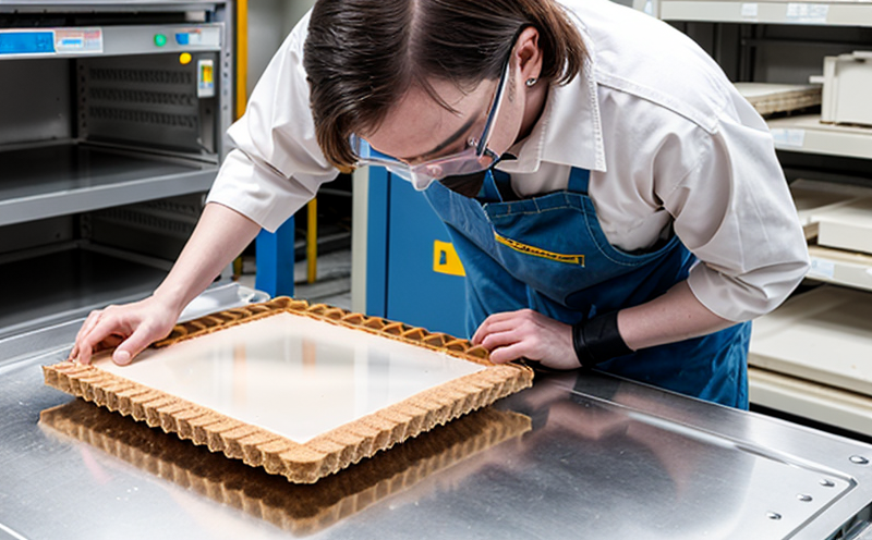
ASTM F1291 Wafer Surface Topography Testing
The ASTM F1291 standard provides a comprehensive framework for assessing wafer surface topography, which is critical in semiconductor and microchip manufacturing. This testing ensures that wafers meet the stringent requirements necessary to support high-performance integrated circuits and advanced electronics. The process involves detailed characterization of the wafer's surface using various metrology tools, ensuring that any defects or irregularities are identified early in the production cycle.
The primary aim is to ensure that each wafer adheres to the design specifications set by the manufacturer. This includes not only the overall flatness but also the uniformity of the surface across its entirety. Variations in topography can lead to performance inconsistencies, affecting the reliability and longevity of the final product.
ASTM F1291 specifies a number of parameters that must be measured and reported, including:
- Absolute flatness
- Surface roughness (Ra)
- Surface roughness (Rz)
- Defects such as scratches or pits
The testing process begins with thorough preparation of the wafer, ensuring it is clean and free from contaminants. This is achieved through a series of cleaning steps using solvents and ultrasonic baths. Once cleaned, the wafer undergoes metrology analysis to measure its surface characteristics.
The metrology instruments used include atomic force microscopes (AFM), optical profilometers, and stylus profilometers. These tools provide high-resolution images and data that are crucial for evaluating the topography of the wafer's surface. The collected data is then analyzed using statistical methods to ensure compliance with ASTM F1291 standards.
The results of this testing are critical in quality assurance processes, helping manufacturers identify potential issues early on. This not only improves product quality but also reduces costs associated with rework or scrap. Compliance with ASTM F1291 is essential for ensuring that the wafers meet the stringent requirements set by semiconductor and electronics industries.
| Standard | Description |
|---|---|
| ASTM F1291-18 | Specification for Surface Topography of Silicon Wafers |
| ISO 4287:2017 | Surface Texture - Profile Method |
| EN ISO 4287:2017 | Surface Texture - Profile Method |
The testing process is highly repeatable and reproducible, ensuring that every wafer undergoes the same rigorous examination. This consistency is vital for maintaining high standards in semiconductor manufacturing.
Applied Standards
The ASTM F1291 standard ensures uniformity in the testing methodology across different manufacturers and laboratories, contributing to a more standardized approach in the industry. The application of these standards is critical for ensuring that each wafer meets the stringent requirements set by semiconductor and electronics industries.
Quality and Reliability Assurance
The ASTM F1291 testing process plays a crucial role in quality assurance (QA) and reliability assurance (RA). By identifying defects early in the production cycle, manufacturers can improve product quality and reduce costs associated with rework or scrap. This ensures that the final products are reliable and perform as expected under various operating conditions.
The testing process is not just about meeting standards; it's also about ensuring long-term reliability of the devices manufactured on these wafers. By adhering to ASTM F1291, manufacturers can demonstrate their commitment to producing high-quality products that meet global industry benchmarks.
International Acceptance and Recognition
The ASTM F1291 standard is widely recognized and accepted in the semiconductor and electronics industries. This broad recognition ensures that manufacturers can confidently use this testing method to meet global standards, thereby expanding their market reach.
Many international laboratories comply with ASTM F1291, ensuring consistency and reliability across different regions. This acceptance by major players in the industry further reinforces its importance as a benchmark for quality assurance.


