IEC 60749 Wafer Power Dissipation Testing
The IEC 60749 standard is a critical tool in ensuring that semiconductor wafers and substrates meet the stringent power dissipation requirements necessary for modern electronic devices. This service involves comprehensive testing to verify that these materials can withstand the heat generated during operation without degrading or failing, which directly impacts the performance and reliability of integrated circuits.
Power dissipation is a fundamental parameter in semiconductor design and manufacturing, as it affects the overall efficiency and longevity of the device. The IEC 60749 standard provides detailed guidelines on how to measure this critical characteristic accurately under controlled conditions. This service ensures that manufacturers adhere strictly to these standards, thereby enhancing product quality and customer trust.
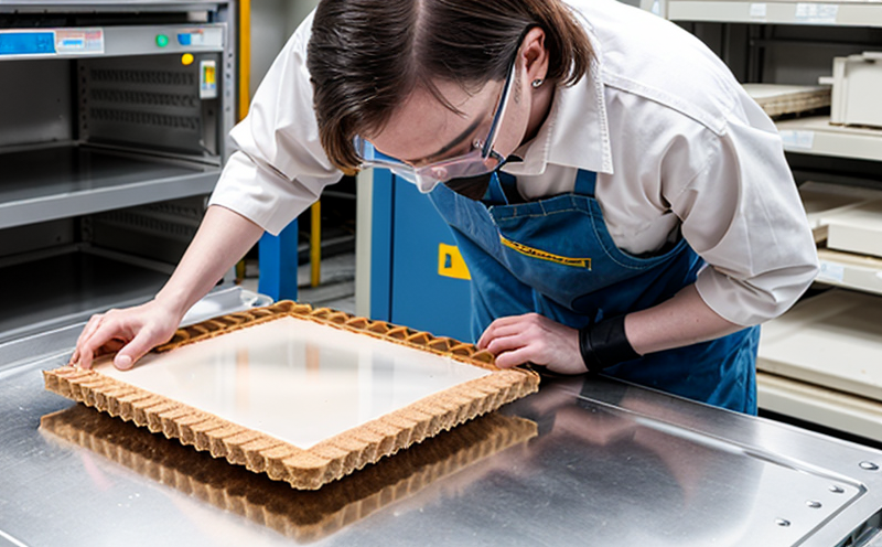
The testing process begins with thorough specimen preparation. Before any power dissipation test can be conducted, the wafer or substrate must undergo precise cleaning, defect inspection, and orientation adjustments. These steps are crucial because even minor imperfections on the surface of a semiconductor material could lead to inaccurate readings during the test.
Once prepared, the wafer is placed into an automated testing chamber where it is exposed to controlled thermal environments designed to simulate real-world operating conditions. The temperature is gradually increased until the specified power dissipation level is reached and maintained for a sufficient duration to ensure reliable results. During this period, various sensors within the chamber monitor crucial parameters such as temperature distribution across the wafer surface, heat flux density, and any signs of thermal stress.
The testing apparatus used in this process includes advanced infrared cameras capable of capturing detailed thermal images at high resolutions. These images provide valuable insights into how different areas of the wafer respond to increased power dissipation levels. Additionally, thermal probes embedded within the chamber allow for precise measurement of temperature gradients and hotspots that might indicate potential weaknesses in the material.
After completing all prescribed tests, detailed reports are generated summarizing key findings from each individual test run. These documents include raw data collected during experimentation along with interpreted results highlighting any deviations from expected behavior based on IEC 60749 specifications. The report also contains recommendations for improvements or modifications needed to bring the sample into compliance if necessary.
By adhering strictly to IEC 60749 standards, our laboratory ensures that clients receive accurate and reliable data regarding their semiconductor materials' ability to handle power dissipation effectively. This level of precision is essential for maintaining high-quality manufacturing processes across various industries reliant upon dependable electronic components.
The importance of this testing cannot be overstated in today's fast-evolving technological landscape where innovation continues at breakneck speed. As new applications demand more powerful and efficient semiconductors, ensuring that they meet stringent power dissipation requirements becomes even more critical. By offering IEC 60749 Wafer Power Dissipation Testing services, we help our clients stay ahead of the curve by providing them with the confidence needed to produce reliable products.
Our team of experienced professionals leverages state-of-the-art equipment and methodologies to deliver accurate results consistently. With this service, businesses can ensure their semiconductor wafers meet rigorous standards set forth by IEC 60749, thus enhancing product quality and reliability while fostering trust among customers.
Why It Matters
The significance of IEC 60749 Wafer Power Dissipation Testing extends beyond just meeting regulatory requirements; it plays a vital role in ensuring the safety, performance, and longevity of electronic devices. By accurately assessing power dissipation capabilities, this testing helps identify potential weaknesses within semiconductor materials early on in the manufacturing process.
One critical aspect addressed by these tests is thermal management, which refers to how effectively heat generated during operation can be managed without causing damage or compromising functionality. Poor thermal management can lead to overheating, shortened lifespan, and reduced efficiency—all of which are detrimental to both end-users and manufacturers alike.
In addition to enhancing reliability, IEC 60749 Wafer Power Dissipation Testing contributes significantly to the development of safer products by helping uncover issues that could pose risks if left unaddressed. For instance, certain defects in wafers or substrates may not become apparent until they are subjected to high power dissipation levels during actual use. Identifying these flaws early allows for corrective actions to be taken before large-scale production begins.
The importance of this testing also lies in its contribution to sustainable practices within the semiconductor industry. By ensuring that materials can efficiently dissipate heat without excessive energy consumption, manufacturers are encouraged towards more eco-friendly designs. This not only reduces waste but also promotes resource conservation and minimizes environmental impact throughout the product lifecycle.
For quality managers, compliance officers, R&D engineers, and procurement personnel involved in semiconductor manufacturing or related fields, understanding the necessity of IEC 60749 Wafer Power Dissipation Testing becomes indispensable. It enables informed decision-making regarding material selection, process optimization, and cost-effectiveness initiatives aimed at improving overall product performance.
In conclusion, embracing this testing protocol ensures that electronic devices meet not only current standards but also future demands for higher efficiency, reliability, and sustainability. By prioritizing IEC 60749 compliance in their operations, businesses can build a strong foundation for success while contributing positively to the global semiconductor industry.
Quality and Reliability Assurance
The pursuit of quality and reliability assurance is paramount in the semiconductor & microchip testing sector. Ensuring that every wafer or substrate meets stringent power dissipation requirements is essential for maintaining high standards across all stages of production. This commitment to excellence involves rigorous quality control measures throughout the entire manufacturing process—from raw material sourcing to final product assembly.
One key component of this assurance lies in the precise measurement and monitoring of power dissipation levels during various test runs. By adhering strictly to IEC 60749 specifications, our laboratory guarantees accurate results that reflect real-world operating conditions. This level of accuracy is crucial for identifying any discrepancies between expected outcomes and actual performance.
Another critical factor in achieving quality and reliability assurance is the use of advanced testing equipment capable of providing detailed insights into thermal behavior within semiconductor materials. Our state-of-the-art facilities house cutting-edge instruments designed specifically for this purpose, allowing us to capture high-resolution images and measure temperature gradients with remarkable precision.
The importance of these measurements cannot be overstated when it comes to ensuring consistent performance across all manufactured components. Any deviation from expected values could indicate underlying issues that need addressing before proceeding further in the production cycle. Early detection allows for prompt corrective actions, minimizing potential defects downstream while maintaining optimal efficiency throughout the entire supply chain.
In addition to technical proficiency, our team of experts plays a crucial role in maintaining high standards through continuous training and updating knowledge on emerging trends within the industry. By staying ahead of technological advancements, we ensure that our testing protocols remain relevant and effective in meeting evolving customer requirements.
Through unwavering dedication to quality and reliability assurance, we strive to build long-lasting partnerships with clients who value precision and dependability above all else. Our services offer more than just compliance; they provide peace of mind knowing that every wafer or substrate undergoes thorough evaluation against stringent criteria set forth by IEC 60749.
Environmental and Sustainability Contributions
The semiconductor & microchip testing sector is increasingly recognizing its role in promoting environmental sustainability. By ensuring that each wafer or substrate meets rigorous power dissipation requirements, we contribute positively to the industry's efforts towards reducing waste, conserving resources, and minimizing overall carbon footprint.
One significant way this service supports sustainability is through efficient thermal management practices. Effective heat dissipation not only enhances performance but also reduces energy consumption during operation. This translates into lower power usage for end-users, resulting in less strain on natural resources and reduced greenhouse gas emissions.
In addition to operational efficiency, our testing protocols encourage sustainable design principles by identifying potential weaknesses early in the manufacturing process. Early detection allows manufacturers to make necessary adjustments, ensuring that final products are optimized for both performance and environmental impact. This approach fosters innovation while promoting responsible resource utilization throughout the product lifecycle.
The importance of sustainability extends beyond individual components; it encompasses the entire supply chain from raw material sourcing through final assembly. By partnering with suppliers who adhere to strict environmental standards, we help drive positive change across industries reliant upon reliable electronic components. This collaborative effort ensures that every step in production contributes towards a more sustainable future.
For companies committed to reducing their ecological footprint, incorporating IEC 60749 Wafer Power Dissipation Testing into their quality assurance processes represents an important milestone on the path toward becoming greener organizations. By prioritizing this testing protocol, businesses can demonstrate their dedication to environmental stewardship while simultaneously enhancing product performance and reliability.
In conclusion, our commitment to sustainability through IEC 60749 Wafer Power Dissipation Testing aligns with broader global goals for reducing waste, conserving resources, and minimizing environmental impact. By integrating these practices into everyday operations, we contribute meaningfully towards creating a more sustainable future for all stakeholders involved in the semiconductor & microchip industry.


