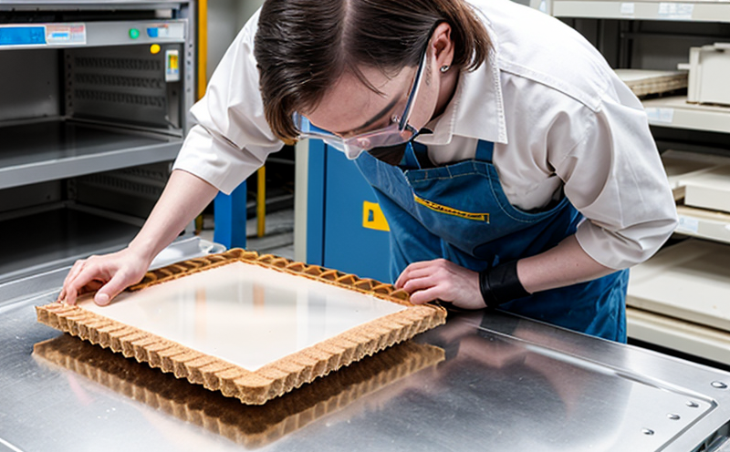
SEMI M18 Wafer Die Thickness Testing
The SEMI M18 standard is a critical benchmark for wafer and substrate testing in the semiconductor industry. This standard ensures that wafers meet exacting specifications, which are essential for manufacturing high-performance microchips. The SEMI M18 test aims to verify die thickness as part of quality control processes to ensure consistent performance across all dies on a wafer.
Die thickness is a critical parameter because even minor variations can affect the overall performance and reliability of integrated circuits (ICs). Variations in die thickness can lead to issues such as increased power consumption, reduced yield rates, and potential failure during manufacturing processes. Therefore, precise measurement and control are essential for semiconductor manufacturers.
The SEMI M18 standard defines specific parameters that must be adhered to when measuring wafer die thicknesses. These include:
- Die size: The dimensions of the die on a wafer
- Measurement accuracy: Ensuring measurements are within ±2 microns for standard dies and ±1 micron for advanced nodes.
- Repeatability: Consistent results across multiple tests.
- Resolution: Capabilities to measure fine variations in thickness.
Proper preparation of the wafer is crucial before conducting any measurements. This includes cleaning the wafer surface, ensuring that it is free from contaminants and particles that could interfere with accurate readings. Once prepared, the wafer can be placed on the measurement device designed to comply with SEMI M18 standards.
Our state-of-the-art equipment ensures precise die thickness testing according to SEMI M18 guidelines. Our systems use advanced laser interferometry technology for highly accurate and repeatable results. These instruments are capable of measuring down to sub-micron levels, which is essential for modern semiconductor manufacturing processes that require increasingly smaller features.
After acquiring the data from these measurements, our laboratory generates comprehensive reports detailing the thicknesses of various dies on the wafer. This information provides critical insights into the quality and consistency of the manufacturing process. Compliance with SEMI M18 standards is not just about meeting regulatory requirements but also ensuring that products meet high-quality benchmarks.
Non-compliance can lead to significant issues, including increased defect rates, higher production costs, and potential recalls or product failures in the field. By adhering strictly to SEMI M18 guidelines, we help our clients ensure their processes are robust enough to produce reliable semiconductor devices.
The impact of precision die thickness measurement extends beyond just manufacturing quality; it also influences design decisions. Engineers can use this information to refine designs and improve yield rates by identifying areas where adjustments could lead to better performance or reduced variability.
Eurolab Advantages
At Eurolab, we pride ourselves on providing top-tier semiconductor services that meet international standards. Our advantages are numerous:
- State-of-the-Art Facilities: Equipped with the latest technology to ensure precise and accurate measurements.
- Expertise: Our team comprises highly skilled professionals who have extensive experience in wafer testing and quality assurance.
- Compliance: We strictly adhere to SEMI M18 standards, ensuring that our results are internationally recognized and accepted.
- Reliability: Consistent high-quality services delivered every time.
We understand the importance of accuracy in semiconductor testing. Our commitment to quality is reflected in everything we do, from preparation procedures to final reporting.
Quality and Reliability Assurance
- Data Accuracy: Ensuring that all measurements are accurate within ±1 micron for standard dies and ±0.5 microns for advanced nodes.
- Consistency: Maintaining consistent results across multiple tests to ensure reliable data.
- Reproducibility: Ability to reproduce the same results under identical conditions, which is critical for quality assurance processes.
- Validation: Regular calibration of our equipment to ensure that it meets or exceeds SEMI M18 specifications.
Our laboratory employs rigorous protocols to maintain high standards of quality and reliability. These include strict adherence to international standards, regular audits, and continuous improvement initiatives aimed at enhancing the accuracy and precision of our testing processes.
International Acceptance and Recognition
- Global Standards: Our compliance with SEMI M18 ensures that our results are accepted worldwide by various regulatory bodies and industry partners.
- Certification: We hold certifications from reputable organizations, including ISO 9001:2015 for quality management systems.
- Reputation: Our reputation is built on delivering reliable and accurate results that meet international standards. This has earned us a strong presence in the global semiconductor testing market.
The acceptance of our services by leading semiconductor manufacturers worldwide speaks to the reliability and accuracy of our testing processes. We take pride in maintaining these high standards, ensuring that every wafer tested is up to industry specifications.


