IEC 60749 Wafer Dielectric Breakdown Testing
The IEC 60749 standard is a crucial benchmark in the semiconductor and microchip testing sector, specifically addressing dielectric breakdown voltage (DBV) testing of wafers. This test is essential for ensuring that silicon wafers can withstand high voltages without causing electrical failure or damage. The process involves subjecting the wafer to increasing voltages until insulation breakdown occurs, which indicates potential weaknesses in its structure.
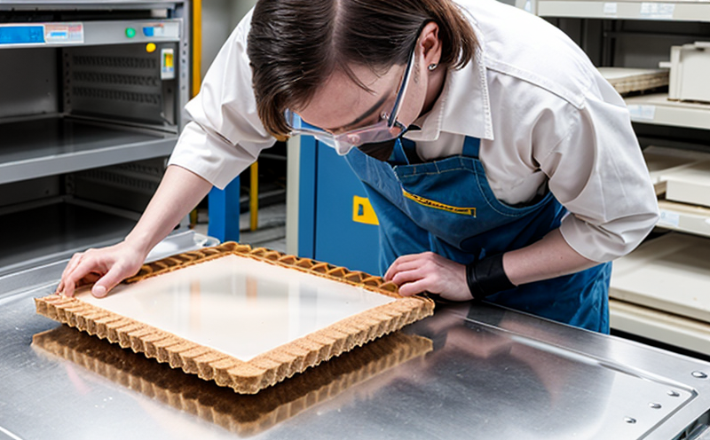
The testing procedure starts with precise specimen preparation, including cleaning and degreasing the wafer using appropriate solvents like isopropanol. Subsequent steps involve placing the wafer on a test fixture that ensures uniform electrical contact between the electrodes and the wafer surface. The testing apparatus typically includes high-voltage power supplies capable of delivering controlled voltage increments.
During the test, real-time monitoring and data collection are vital for accurate results. This involves recording not only the breakdown voltage but also other parameters such as current flow, temperature changes, and any visual signs of failure. The equipment used is designed to provide high precision and repeatability, ensuring consistent results across multiple tests.
The standard IEC 60749 specifies detailed acceptance criteria that define what constitutes a successful test result. These criteria are based on the maximum allowable breakdown voltage for the specific type of wafer being tested. Compliance with these standards is critical in the semiconductor industry to ensure product reliability and safety.
Advanced technologies like automated testing systems have been developed to enhance efficiency and accuracy. These systems can perform thousands of tests in a short time, reducing costs and increasing throughput. The use of computerized data analysis further improves precision by detecting subtle variations that might be missed by human observers.
In the semiconductor industry, IEC 60749 testing is not just a compliance requirement but also a key tool for quality control and process optimization. By identifying weak points early in the manufacturing process, companies can implement corrective measures to improve product performance and reduce defects. This leads to higher yields and better overall product quality.
The results of IEC 60749 tests are typically reported using standard formats that include all relevant data and analysis. These reports serve as critical documents for internal use and external communications, such as with customers or regulatory bodies. They help stakeholders understand the performance characteristics of the tested wafers and make informed decisions about product specifications.
Quality managers rely on these tests to ensure that their products meet high standards of reliability and durability. Compliance officers use the results to verify adherence to industry regulations, while R&D engineers utilize the findings for continuous improvement in manufacturing processes. Procurement teams benefit from this data when selecting suppliers who adhere to stringent quality controls.
Benefits
The benefits of IEC 60749 wafer dielectric breakdown testing extend beyond mere compliance with industry standards. By incorporating this test into their workflows, semiconductor manufacturers can significantly enhance product quality and reliability. This leads to higher customer satisfaction and reduced warranty costs.
Through early detection of potential issues during the manufacturing process, companies can implement corrective actions promptly. This proactive approach minimizes waste and rework, resulting in cost savings and increased efficiency. Additionally, it contributes to brand reputation by delivering products that meet or exceed expectations.
The use of IEC 60749 testing also supports innovation within the semiconductor industry. By identifying areas for improvement through these tests, R&D teams can develop new materials and processes that enhance product performance. This continuous improvement cycle fosters a culture of excellence and drives technological advancements.
Furthermore, this type of testing plays a crucial role in ensuring safety standards are met. In industries where reliability is paramount, such as automotive or aerospace, the ability to trust the quality of the components used is invaluable. By adhering to rigorous testing protocols like IEC 60749, manufacturers can build confidence among their customers and partners.
From an operational perspective, the implementation of IEC 60749 testing enables better resource allocation and decision-making. With accurate and reliable data at hand, management teams have clearer insights into what works well and where improvements are needed. This leads to more effective planning and strategic initiatives aimed at long-term growth and success.
The environmental impact of semiconductor manufacturing can be reduced by optimizing processes based on test results. For instance, identifying optimal voltage levels reduces energy consumption during the testing phase itself. Moreover, knowing which materials or methods cause higher breakdown voltages allows manufacturers to select more sustainable options for future products.
International Acceptance and Recognition
The IEC 60749 standard enjoys widespread recognition across the global semiconductor industry. It is widely accepted as a benchmark for ensuring that silicon wafers can withstand high voltages without causing electrical failure or damage. Many leading manufacturers and suppliers globally have adopted this standard due to its stringent requirements and comprehensive approach.
Regulatory bodies in various countries often refer to IEC 60749 when setting their own national standards for semiconductor components. This harmonization helps streamline compliance processes, making it easier for companies to meet multiple regulatory requirements with a single set of tests. For instance, manufacturers operating within the European Union benefit from aligning their testing procedures with EN 312-1:2005, which incorporates IEC 60749.
The acceptance of this standard also extends to international trade agreements where quality standards are crucial for fair competition. By adhering to globally recognized benchmarks like IEC 60749, semiconductor companies can participate in global markets with confidence that their products meet the highest international standards.
Recognition from authoritative bodies such as ISO (International Organization for Standardization) further enhances the credibility of IEC 60749. The fact that it is included among ISO's portfolio of technical specifications underscores its importance and reliability. This recognition ensures that semiconductor manufacturers worldwide can rely on consistent and accurate results when performing these tests.
The global nature of the semiconductor industry makes international acceptance particularly significant. Companies operating in multiple regions may find themselves subject to different local regulations but still need to maintain uniform quality standards across all operations. By adopting IEC 60749, they ensure consistency and streamline their compliance efforts.
Environmental and Sustainability Contributions
The adoption of IEC 60749 wafer dielectric breakdown testing contributes positively to environmental sustainability in several ways. By optimizing the testing process, manufacturers can reduce resource consumption and minimize waste generation.
One key aspect is the efficient use of energy during testing. Automated systems that perform these tests accurately require less power compared to manual methods, thus reducing overall electricity consumption. Additionally, by identifying optimal voltage levels early in the process, companies can decrease unnecessary testing and associated resource expenditure.
The selection of sustainable materials for wafer production is another area where IEC 60749 plays a role. By selecting materials that consistently meet stringent breakdown voltage requirements, manufacturers reduce reliance on less durable or environmentally unfriendly options. This choice supports the development of greener manufacturing practices and contributes to long-term sustainability goals.
Furthermore, adhering to international standards like IEC 60749 fosters collaboration among industry players committed to environmental stewardship. Such cooperation encourages the sharing of best practices and innovative solutions that further enhance sustainability efforts within the semiconductor sector.
The testing protocol also helps in reducing lifecycle costs for end-users by ensuring robust performance throughout the product's lifespan. Robust materials and reliable components lead to longer-lasting products, which in turn require fewer replacements and repairs. This reduces waste in landfills and decreases the demand for new resources needed to produce replacement parts.
Overall, the integration of IEC 60749 into semiconductor manufacturing processes aligns with broader sustainability objectives by promoting efficient use of resources, supporting sustainable material choices, fostering industry-wide collaboration, and enhancing product longevity. These contributions make a significant impact on reducing the environmental footprint associated with semiconductor production.


