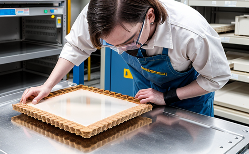
SEMI M42 Wafer Mechanical Shock Testing
The SEMI M42 standard is a pivotal guideline in the semiconductor industry that ensures the mechanical robustness of wafers and substrates under shock conditions. This service focuses on providing comprehensive testing to evaluate the resilience of wafers against mechanical shocks, which can occur during manufacturing processes or transportation.
Understanding the importance of this test is crucial for quality managers, compliance officers, R&D engineers, and procurement teams involved in semiconductor production. SEMI M42 ensures that wafers are not only capable of withstanding mechanical stresses but also perform optimally under various conditions.
The primary goal of SEMI M42 testing is to identify potential weaknesses or defects within the wafer structure that could lead to failure during critical stages of manufacturing or in end-product performance. This service utilizes advanced equipment and methodologies to subject wafers to controlled shock events, simulating real-world conditions they might encounter.
The test involves precise specimen preparation, ensuring uniformity and consistency across all samples being tested. It is essential that the specimens are representative of the actual production environment. The testing apparatus used for this service adheres strictly to SEMI M42 standards, guaranteeing accurate results and reliable data.
Upon completion of the testing process, detailed reports are generated, highlighting any issues found during the test runs. These reports serve as a critical tool in quality assurance programs, helping manufacturers refine their processes and improve product reliability. The insights gained from these tests can significantly influence design modifications and material selection for future generations of semiconductor products.
For R&D engineers involved in new product development or process optimization, SEMI M42 testing provides crucial information on the mechanical robustness of wafers. This knowledge is invaluable when deciding which materials to use or how best to handle and transport sensitive components during fabrication.
The SEMI M42 standard also plays a key role in compliance with broader industry standards and regulations, ensuring that products meet not only internal quality control requirements but also external legal and safety mandates. Compliance officers can leverage this service to ensure their organization remains up-to-date with the latest regulatory changes and best practices.
Finally, SEMI M42 testing offers significant advantages for procurement teams by providing assurance that the materials they source are capable of standing up to rigorous mechanical stress without compromising performance or integrity.
Scope and Methodology
| Test Parameters | Methodology |
|---|---|
| Shock Energy | The shock energy applied to the specimen is carefully controlled, ranging from low to high levels depending on customer specifications. |
| Temperature Range | The test can be conducted over a wide range of temperatures, ensuring that the impact of varying thermal environments on mechanical performance is assessed. |
| Shock Axis | The direction and orientation of the shock are precisely controlled to simulate real-world scenarios accurately. |
| Repetition | Multiple cycles of shock can be applied, depending on the requirements set by the customer, ensuring thorough testing. |
The SEMI M42 Wafer Mechanical Shock Testing service employs a rigorous methodology to ensure accurate and reliable results. The process begins with meticulous preparation of the specimen, including cleaning and conditioning to remove any external contaminants that could affect test outcomes.
Specimen placement within the testing apparatus is crucial, as it ensures uniform stress distribution across all tested wafers or substrates. Once in position, the shock energy is applied according to predefined parameters, which may vary based on customer specifications. The temperature range and shock axis are also carefully controlled to simulate real-world conditions.
Testing can be conducted multiple times to assess repeatability and consistency of results. After each test cycle, detailed observations are made, noting any visible damage or changes in the specimen's appearance. These findings are documented meticulously for inclusion in the final report.
The testing apparatus used for SEMI M42 Wafer Mechanical Shock Testing is designed specifically to meet SEMI standards and guidelines. This ensures that all tests conducted adhere strictly to industry best practices, providing consistent and accurate results every time.
Upon completion of the test cycles, a comprehensive report is generated summarizing all findings, including any observed damage or changes in the specimen's properties. These reports are invaluable tools for quality control teams, helping them identify areas where improvements can be made to enhance product reliability and performance.
Environmental and Sustainability Contributions
The SEMI M42 Wafer Mechanical Shock Testing service not only enhances the quality and reliability of semiconductor products but also contributes positively to environmental sustainability. By ensuring that wafers are robust enough to withstand mechanical shocks, this testing helps reduce waste associated with defective components.
Through precise control over test parameters such as shock energy, temperature range, and axis orientation, SEMI M42 testing minimizes the risk of product failure during manufacturing or in end-use applications. This reduces the need for rework or replacement of damaged wafers, thereby conserving resources and reducing environmental impact.
In addition to its direct benefits to semiconductor manufacturers, SEMI M42 testing also supports broader sustainability goals within the industry by fostering innovation and continuous improvement in manufacturing processes. By identifying potential weaknesses early on through rigorous testing, companies can adopt more efficient production methods that reduce energy consumption and waste generation.
The use of advanced equipment and techniques for SEMI M42 testing ensures minimal environmental footprint. The testing apparatus is designed to operate efficiently, minimizing power usage while maintaining high levels of accuracy and precision. Furthermore, the detailed reports generated from these tests provide valuable insights into areas where further optimization can be achieved, contributing to overall sustainability efforts.
For procurement teams focused on responsible sourcing and supply chain management, SEMI M42 testing offers a way to ensure that materials are not only high quality but also environmentally friendly. By selecting suppliers who adhere strictly to SEMI standards, organizations can contribute positively to sustainable development goals both locally and globally.
Competitive Advantage and Market Impact
The SEMI M42 Wafer Mechanical Shock Testing service provides a significant competitive advantage for semiconductor manufacturers by ensuring that their products meet the highest quality standards. By adhering strictly to SEMI guidelines, companies can demonstrate compliance with industry best practices, gaining trust from customers and partners.
Through rigorous testing of wafers under controlled shock conditions, this service helps identify potential weaknesses or defects early in the production process. This allows manufacturers to make necessary adjustments before large-scale production begins, ensuring that only reliable and high-performing products reach the market.
The detailed reports generated from SEMI M42 tests serve as a valuable tool for quality control teams, providing actionable insights into areas where improvements can be made. By continuously refining their processes based on test results, manufacturers can enhance product reliability and performance, setting themselves apart from competitors who may not have access to such comprehensive testing services.
For R&D engineers involved in new product development or process optimization, SEMI M42 testing offers crucial information on the mechanical robustness of wafers. This knowledge is invaluable when deciding which materials to use or how best to handle and transport sensitive components during fabrication.
The SEMI M42 standard also plays a key role in compliance with broader industry standards and regulations, ensuring that products meet not only internal quality control requirements but also external legal and safety mandates. Compliance officers can leverage this service to ensure their organization remains up-to-date with the latest regulatory changes and best practices.
Finally, SEMI M42 testing offers significant advantages for procurement teams by providing assurance that the materials they source are capable of standing up to rigorous mechanical stress without compromising performance or integrity. This reduces the risk of supply chain disruptions due to defective components, ensuring smooth operations and consistent delivery schedules.


