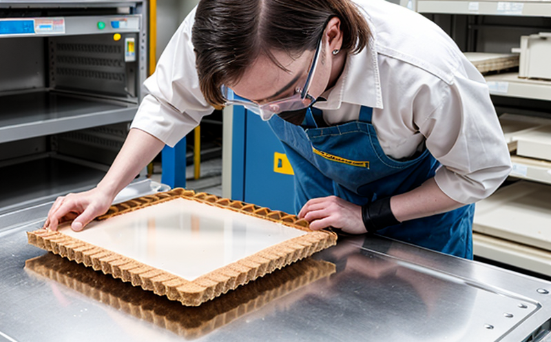
SEMI M20 Silicon Wafer Traceability Marking Testing
The SEMI M20 Silicon Wafer Traceability Marking Testing is a critical step in ensuring that semiconductor wafers are accurately identified and tracked throughout the manufacturing process. This testing ensures compliance with industry standards, particularly those outlined by the Semiconductor Equipment and Materials International (SEMI), which is pivotal for quality assurance and supply chain management.
The SEMI M20 standard mandates the use of specific marking techniques to uniquely identify each silicon wafer. These markings are essential for tracking wafers from their initial stages through multiple processing steps, including cleaning, etching, doping, and thinning. The testing process involves several key components that ensure the integrity and reliability of the markings:
- Marking accuracy
- Depth uniformity
- Positional precision
- Readable contrast
- Durability over subsequent processing steps
The testing process typically involves the following steps:
- Preparation of Samples: Wafers are carefully prepared by ensuring they are free from contaminants and defects that could interfere with marking accuracy.
- Marking Process: Various marking techniques such as laser etching, ink printing, or photoresist application are used to create the required markings. The specific technique depends on the subsequent processing steps of the wafer.
- Inspection and Testing: Once marked, wafers undergo a series of non-destructive inspections using high-resolution microscopy and laser scanning techniques to ensure that all marking criteria have been met. This includes checking for any imperfections or inconsistencies in the marking process.
This testing is not only about ensuring compliance with SEMI M20 standards but also plays a crucial role in enhancing traceability within the semiconductor industry. By accurately identifying each wafer, manufacturers can better manage inventory, reduce errors in processing steps, and improve overall quality control. This leads to more reliable end products that meet stringent performance requirements.
The importance of this testing cannot be overstated. In an industry where even minor discrepancies can lead to significant financial losses and reputational damage, SEMI M20 compliance is essential. By adhering to these standards, manufacturers can ensure that their processes are consistent, efficient, and capable of producing high-quality products.
Moreover, the testing process also supports broader industry initiatives aimed at improving supply chain transparency and sustainability. By accurately tracking each wafer from its point of origin through various stages of production, manufacturers can better manage resources, reduce waste, and contribute to a more sustainable manufacturing environment.
Why It Matters
The SEMI M20 Silicon Wafer Traceability Marking Testing is not just a compliance requirement but also a critical enabler of efficient and reliable semiconductor production. Here are several reasons why this testing matters:
- Avoidance of Errors: Accurate marking ensures that each wafer can be traced back to its initial processing steps, minimizing the risk of errors in subsequent stages.
- Enhanced Quality Control: By ensuring that all wafers meet strict marking criteria, this testing contributes significantly to overall product quality and reliability.
- Informed Decision-Making: Accurate traceability allows manufacturers to make informed decisions about process improvements and resource allocation.
- Improved Supply Chain Management: Enhanced traceability supports better supply chain management by providing clear visibility into the movement of materials and products.
The SEMI M20 standard is widely recognized as a best practice in the semiconductor industry. By adhering to this standard, manufacturers can ensure that their processes are consistent and reliable, leading to higher-quality end products and increased customer satisfaction.
Moreover, compliance with these standards is not just beneficial for individual companies but also contributes to the broader industry’s goals of improving efficiency and sustainability. Accurate traceability helps in reducing waste, optimizing resource use, and minimizing environmental impact.
Industry Applications
- Wafer Fabrication: Ensures that each wafer can be accurately traced back to its initial processing steps, facilitating quality control and error prevention.
- Chip Manufacturing: Supports the production of high-quality chips by ensuring consistent marking processes across all stages of manufacturing.
- Silicon Wafer Supply Chain Management: Enhances traceability throughout the supply chain, improving inventory management and reducing errors in processing steps.
- Quality Assurance: Guarantees that each wafer meets strict quality standards, leading to higher-quality end products.
The SEMI M20 standard is particularly important for large-scale semiconductor manufacturers who rely on consistent and reliable processes. By adhering to these standards, they can ensure that their products meet the highest quality standards and are capable of withstanding rigorous testing and performance requirements.
Furthermore, this testing supports broader industry initiatives aimed at improving supply chain transparency and sustainability. Accurate traceability helps in reducing waste, optimizing resource use, and minimizing environmental impact, contributing to a more sustainable manufacturing environment.
Eurolab Advantages
Eurolab offers comprehensive SEMI M20 Silicon Wafer Traceability Marking Testing services that provide a range of advantages for our clients:
- Expertise and Experience: Our team of experts has extensive experience in semiconductor testing, ensuring accurate and reliable results.
- State-of-the-Art Equipment: We use the latest instrumentation to ensure precise marking and comprehensive inspections.
- Comprehensive Testing Capabilities: We offer a full suite of testing services, covering all aspects of SEMI M20 compliance.
- Rapid Turnaround Time: Our efficient processes allow for quick turnaround times, minimizing downtime in the production line.
- Compliance and Quality Assurance: By ensuring strict adherence to SEMI M20 standards, we help our clients maintain high-quality standards and ensure compliance with industry regulations.
- Customer Support: Our dedicated customer support team is available to assist clients with any questions or concerns throughout the testing process.
Eurolab’s commitment to quality and expertise ensures that our clients can trust us to deliver reliable and compliant results. Whether you are a small-scale manufacturer or a large semiconductor company, Eurolab offers the support and services needed to ensure accurate marking and traceability of your silicon wafers.


