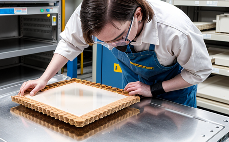
SEMI M34 Wafer Surface Geometry Testing
The SEMI M34 Standard outlines a method for wafer surface geometry testing. This test is critical in the semiconductor and microchip manufacturing process as it ensures that wafers meet dimensional accuracy requirements, which are paramount to the successful fabrication of integrated circuits. Compliance with this standard helps manufacturers maintain consistent quality across production batches.
Wafer surface geometry testing involves measuring various parameters such as wafer flatness, warp, and thickness variations using specialized equipment like laser interferometers or optical profilometers. These measurements play a crucial role in the early detection of defects that could lead to yield losses downstream in the manufacturing process. By adhering to SEMI M34, manufacturers can ensure their processes meet industry best practices and regulatory requirements.
The SEMI M34 standard provides detailed procedures for testing wafer surface geometry, including pre-test preparation steps like cleaning the wafer and calibrating the equipment. Post-test analysis involves comparing measured values against specified tolerances outlined in the standard. This ensures that any deviations from acceptable limits are identified promptly.
The importance of SEMI M34 cannot be overstated for modern semiconductor manufacturing processes. In environments where even minor imperfections can result in significant financial losses, rigorous adherence to these standards is essential. The SEMI M34 standard not only helps maintain process control but also contributes to reducing waste and improving overall productivity.
Wafer surface geometry testing is typically performed at critical stages during the manufacturing cycle, such as after polishing or before etching. These tests help identify potential issues early in the process, allowing for corrective actions to be taken before they lead to costly rework or scrap. By integrating SEMI M34 into their quality assurance protocols, manufacturers can enhance their ability to produce high-quality semiconductor devices consistently.
It's worth noting that while SEMI M34 focuses primarily on wafer surface geometry, it also provides guidance on related parameters like bow and curvature. Understanding these factors helps ensure that wafers are suitable for further processing steps without compromising the integrity of the device being fabricated. This comprehensive approach ensures that manufacturers can achieve optimal results throughout their production lines.
Adhering to SEMI M34 standards is particularly important given the increasing complexity and size of modern semiconductor devices. As feature sizes continue to shrink, maintaining precise control over wafer geometry becomes even more challenging but also more critical for success in this highly competitive industry.
Scope and Methodology
| Parameter | Description |
|---|---|
| Laser Interferometer Measurements | Used to measure wafer flatness, warp, and thickness variations. |
| Optical Profilometers | Measure surface roughness and defect density. |
| Calibration Procedures | Ensure accuracy by regularly calibrating instruments before each test run. |
| Data Analysis | Compare measured values against SEMI M34 specified tolerances. |
Industry Applications
The SEMI M34 standard finds application across various sectors within the semiconductor industry, including foundries, packaging plants, and design houses. Manufacturers rely on this standard to ensure their processes are aligned with international best practices and regulatory requirements.
In production environments where even minor deviations can result in significant financial losses, SEMI M34 helps maintain process control. Early detection of defects through rigorous testing ensures that issues are addressed before they escalate into more severe problems further down the line. This proactive approach contributes to enhancing overall productivity and reducing waste.
The standard's emphasis on precise measurement techniques is particularly beneficial in high-volume manufacturing settings where consistent quality is essential for meeting customer expectations. By adhering to SEMI M34, companies can demonstrate their commitment to excellence and reliability, thereby building trust with customers and partners alike.
Environmental and Sustainability Contributions
The SEMI M34 standard supports environmental sustainability by promoting efficient use of resources throughout the semiconductor manufacturing process. By minimizing waste and optimizing production yields, compliance with this standard helps reduce energy consumption and raw material usage.
Through precise measurement techniques like those outlined in SEMI M34, manufacturers can identify potential inefficiencies early on, allowing for timely adjustments that lead to more sustainable operations. This focus on reducing waste also translates into cost savings for the company while contributing positively to environmental conservation efforts globally.
Moreover, by ensuring high-quality products from the outset, SEMI M34 helps prevent rework and scrap, which are significant contributors to resource depletion in manufacturing processes. The standard's emphasis on continuous improvement encourages ongoing efforts towards greener practices within the semiconductor industry.


