IEC 60749 Wafer Thermal Shock Resistance Testing
The IEC 60749 standard is a critical benchmark for ensuring that semiconductor wafers and substrates can withstand rapid temperature changes without compromising their integrity. This test evaluates the thermal shock resistance of wafers by subjecting them to extreme temperature fluctuations, simulating real-world conditions during manufacturing and use. Semiconductor devices are highly sensitive to thermal stress, making this form of testing essential for quality assurance.
During IEC 60749 testing, a wafer is exposed to a controlled sequence of temperature changes that simulate the rapid heating and cooling cycles it may encounter in production or during device operation. The test involves precise control over environmental conditions, ensuring reproducibility and accuracy. This method helps identify potential weaknesses in the wafer's structure, such as cracks or delamination, which could otherwise lead to failures in subsequent manufacturing steps or operational issues.
The IEC 60749 standard is particularly important for manufacturers of advanced semiconductor devices like power semiconductors and logic chips. By adhering to this standard, companies can ensure that their products meet stringent quality requirements and are reliable under various temperature conditions. This testing process not only enhances product performance but also contributes to the overall reliability and longevity of electronic components.
Wafer thermal shock resistance is a key factor in determining the robustness of semiconductor devices. The ability of a wafer to withstand sudden changes in temperature can significantly impact its usability in harsh environments, such as automotive electronics or industrial applications where extreme conditions are common. Ensuring that wafers meet IEC 60749 standards helps manufacturers deliver products that not only perform well under normal operating conditions but also endure unexpected stressors without failure.
The testing procedure typically involves placing the wafer in a controlled environment and subjecting it to rapid temperature cycling. The rate of change is critical, as excessive or insufficient heating can lead to inaccurate results. Once the desired temperatures are reached, the wafer remains at that temperature for a specified period before being rapidly cooled or heated again. This cycle may be repeated several times to simulate the stress a device might experience during its lifetime.
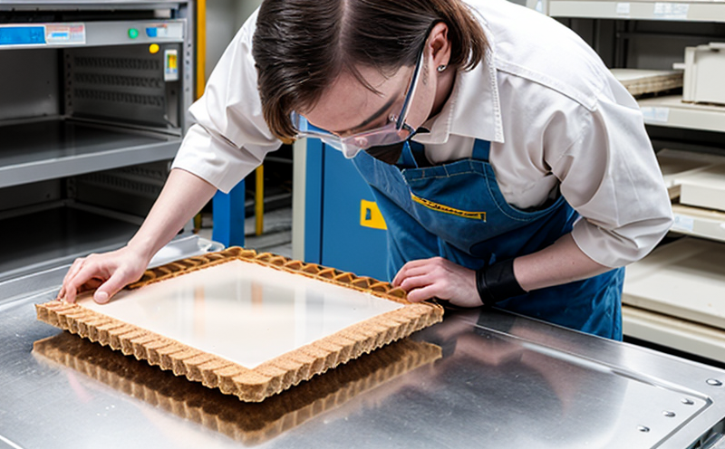
Preparing the specimen for IEC 60749 testing involves careful selection and handling. The wafer must be free from defects, as even minor imperfections could affect test outcomes. Proper cleaning and preparation are crucial to ensure accurate results. Once prepared, the wafer is placed into a thermal shock tester, where it undergoes the prescribed temperature cycling protocol.
The equipment used for this testing includes specialized thermal shock testers that can achieve rapid temperature changes with high precision. These machines are capable of maintaining strict control over temperature and humidity levels throughout the test process. The use of such advanced instrumentation ensures that the results are both reliable and reproducible, providing valuable insights into the wafer's ability to withstand thermal stress.
Accurate reporting is essential in ensuring compliance with IEC 60749 standards. Reports should detail the temperature cycles applied during testing, including start and end points, as well as any deviations from expected behavior. Additionally, visual inspection results and any evidence of defects or damage are documented. These comprehensive reports provide critical information for quality assurance teams and R&D engineers to make informed decisions about process improvements or design modifications.
Adhering to IEC 60749 standards is crucial not only for compliance but also for maintaining a competitive edge in the semiconductor industry. By ensuring that wafers meet these rigorous testing criteria, manufacturers can demonstrate their commitment to quality and reliability. This not only enhances customer confidence but also fosters long-term relationships with suppliers and partners.
The IEC 60749 standard is widely recognized as a benchmark for thermal shock resistance in semiconductor manufacturing processes. Its application ensures that products are robust enough to handle the demanding conditions encountered during production and operation. This testing process plays a vital role in enhancing product performance, reliability, and longevity, making it an indispensable tool for any company involved in the development and production of advanced semiconductor devices.
Why It Matters
The IEC 60749 standard is essential for ensuring that wafers used in semiconductor manufacturing are capable of withstanding rapid temperature changes. This capability is crucial because it directly impacts the reliability and performance of the final electronic devices produced from these wafers. For instance, automotive electronics often operate in environments where temperature fluctuations occur frequently, requiring components that can handle such conditions without failure.
By incorporating IEC 60749 testing into their quality assurance protocols, manufacturers can identify potential issues early on, allowing for corrective actions to be taken before production begins. This proactive approach helps prevent costly rework and ensures a consistent supply of high-quality wafers that meet industry standards.
The standard also plays a pivotal role in fostering innovation within the semiconductor sector. As technology continues to advance, so too do the demands placed on materials used in manufacturing processes. By adhering to IEC 60749 guidelines, researchers and engineers can push the boundaries of what is possible while ensuring that their innovations are robust enough for real-world applications.
Moreover, compliance with this standard contributes significantly to maintaining a high level of trust among consumers who rely on dependable electronic devices. When manufacturers commit to meeting IEC 60749 requirements, they signal their dedication to producing products that can be trusted in any environment. This commitment enhances brand reputation and builds customer confidence.
In conclusion, the importance of IEC 60749 wafer thermal shock resistance testing cannot be overstated. It serves as a crucial link between raw materials and finished goods, ensuring that each step along the way adheres to strict quality controls. As technology evolves, so too must our methods for assessing material performance; by embracing standards like IEC 60749, we pave the way for continued progress in semiconductor manufacturing.
Benefits
Enhances product reliability and durability through rigorous thermal stress testing.
Identifies potential issues early in the production process to prevent costly rework.
Fosters innovation by allowing manufacturers to push the boundaries of material performance.
Maintains a high level of trust and confidence among consumers who rely on dependable electronic devices.
Ensures compliance with international standards, enhancing brand reputation and market competitiveness.
Supports sustainable practices by minimizing waste associated with defective products during production.
The benefits of conducting IEC 60749 wafer thermal shock resistance testing extend beyond mere quality control. By implementing this standard, manufacturers can gain a competitive advantage in the global market while also contributing positively to environmental sustainability efforts.
Environmental and Sustainability Contributions
The implementation of IEC 60749 standards not only enhances product reliability but also supports broader environmental goals. By ensuring that wafers meet stringent thermal shock resistance requirements, manufacturers are contributing to the reduction of waste associated with defective products during production. This reduces energy consumption and resource use, ultimately leading to more sustainable manufacturing practices.
Furthermore, compliance with international standards like IEC 60749 demonstrates a company's commitment to environmental stewardship. Consumers increasingly seek out environmentally responsible brands, making adherence to such guidelines an important factor in maintaining competitive advantage. The standard also promotes transparency and accountability within the supply chain, encouraging all stakeholders to adopt sustainable practices.
By investing in IEC 60749 testing, manufacturers can contribute positively to global efforts aimed at reducing carbon footprints across various industries. This includes minimizing greenhouse gas emissions from production facilities and optimizing resource usage throughout the entire lifecycle of electronic devices.
In summary, the benefits of incorporating IEC 60749 into semiconductor manufacturing processes extend far beyond mere quality assurance. It supports broader environmental objectives by promoting sustainable practices that reduce waste, conserve resources, and minimize impacts on the environment. Additionally, it strengthens market positioning through compliance with internationally recognized standards while fostering transparency and accountability within supply chains.


