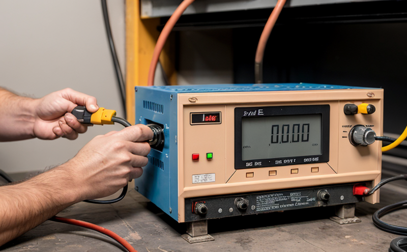
JEDEC JESD22-A123 Die Reverse Bias Stress Testing
The JEDEC JESD22-A123 standard is a critical part of semiconductor and microchip quality assurance. This test assesses the reverse bias breakdown voltage, which measures how much stress can be applied to a diode before it fails. For die-level testing in this context, the focus is on individual components within integrated circuits.
This service involves subjecting silicon dies (pre-assembly) to controlled electrical stresses that simulate real-world operating conditions and potential failure points. The goal is to identify weaknesses or vulnerabilities in the design early in the development cycle, thereby ensuring product reliability and compliance with industry standards.
During this testing procedure, a reverse bias voltage is applied across the diode terminals of the die while monitoring current flow. The test can be conducted at various temperatures to simulate different environmental conditions under which the device might operate. This includes both normal operating temperatures as well as extremes like those found in automotive or aerospace applications.
The results from these tests are crucial for quality assurance teams who rely on them to make informed decisions about product design improvements and manufacturing process adjustments. By identifying issues early, manufacturers can minimize costs associated with late-stage failures during production runs or field use.
For R&D engineers involved in new technology development, this type of testing provides valuable insights into the performance characteristics of novel materials or architectures being considered for future products. It also helps them understand how changes made at the circuit level affect overall system reliability.
The standard is referenced internationally and includes specific criteria that must be met to ensure accurate results. Compliance with these standards not only enhances reputation but also ensures compatibility across different systems, which is essential in today's interconnected technological landscape.
Preparation for this test typically involves careful selection of appropriate test equipment capable of delivering precise voltage levels over a wide range while maintaining stability throughout the duration of each measurement cycle. Specimen preparation usually includes mounting the die onto a suitable holder that allows accurate placement within the testing fixture without compromising its integrity during stress application.
Instrumentation used may vary depending on the specific requirements but generally includes high-precision power supplies, ammeters, and voltmeters capable of operating in low-noise environments. Data acquisition systems are employed to record all relevant parameters throughout each test cycle ensuring comprehensive documentation for analysis purposes later on.
Reporting involves compiling detailed reports summarizing key findings from multiple runs conducted under different conditions if necessary. These documents serve as important references not just during current projects but also future iterations where lessons learned can be applied towards continuous improvement efforts.
Benefits
Conducting JEDEC JESD22-A123 reverse bias stress tests offers several advantages:
- Elevated Product Quality: Identifying defects early in the design phase reduces the risk of field failures and enhances customer satisfaction.
- Cost Savings: By detecting issues before mass production, companies can avoid expensive recalls and warranty claims.
- Enhanced Reliability: Ensuring that components meet or exceed specified performance levels increases confidence in the final product's longevity and reliability.
The ability to perform these tests efficiently contributes significantly to meeting stringent regulatory requirements, thereby fostering trust among end-users who expect high standards from their suppliers.
Competitive Advantage and Market Impact
Implementing JEDEC JESD22-A123 die reverse bias stress testing provides a competitive edge by:
- Maintaining compliance with international standards, thus ensuring compatibility across various platforms.
- Demonstrating a commitment to quality through rigorous testing procedures that exceed industry expectations.
- Allowing early identification and resolution of potential problems before they become costly issues in later stages of development or production cycles.
This service can help companies differentiate themselves from competitors by offering superior products backed by robust evidence of thorough quality assurance practices. It also positions them favorably within the broader semiconductor industry ecosystem, where reliability is paramount for maintaining customer loyalty and fostering long-term business relationships.
Use Cases and Application Examples
| Application Example | Description |
|---|---|
| Automotive Electronics | The reverse bias stress test helps ensure that semiconductors used in automotive systems can withstand the harsh conditions encountered during operation, including extreme temperatures and vibrations. |
| Avionics Systems | In avionics applications where reliability is critical due to life-threatening scenarios, this testing ensures that microchips perform reliably under stress conditions similar to those they might experience in flight environments. |
| Medical Devices | The high-stress environment created by the reverse bias voltage simulates the rigorous operating conditions faced by medical devices used in critical care settings. |
| Data Centers | For data centers, ensuring that semiconductors can handle extreme power surges and other stressors is essential for maintaining optimal performance and preventing downtime. |
- Example 1: In the automotive industry, this test ensures that semiconductors used in braking systems or engine control units can operate reliably under extreme conditions. Without proper testing, there could be risks associated with vehicle safety.
- Example 2: For avionics manufacturers, ensuring their microchips meet stringent reliability standards is crucial for aviation safety. This test helps validate that the chips will perform consistently and safely across a wide range of temperatures and pressures.
Frequently Asked Questions
Die-Level Electrical & Functional Testing Services
- IEC 60747 Semiconductor Die Electrical Parameter Testing
- JEDEC JESD22 Die Functional Characterization Testing
- MIL-STD-883 Method 1010 Die Logic Function Verification Testing
- ASTM F617 Die Breakdown Voltage Measurement Testing
- IEC 60749 Die Leakage Current Electrical Testing
- JEDEC JESD47 Die Burn-in Functional Reliability Testing
- ASTM F723 Die Threshold Voltage Measurement Testing
- IEC 60793 Semiconductor Die Impedance Characterization Testing
- MIL-PRF-38535 Die Electrical Qualification Testing
- ASTM F756 Die Switching Speed Performance Testing
- JEDEC JESD22-A115 Die Input/Output Capacitance Testing
- IEC 62047-8 Micro Die Mechanical Testing
- ASTM F728 Die Microhardness Characterization Testing
- JEDEC JESD22-A114 Die Electrostatic Discharge Testing
- IEC 60749-12 Die Moisture Resistance Electrical Testing
- ASTM F763 Die Interconnect Resistance Testing
- JEDEC JESD22-A104 Die Temperature Cycling Electrical Testing
- IEC 60068 Die Electrical Stress Testing
- ASTM F1249 Die Moisture Permeation Testing
- JEDEC JESD22-A113 Die Preconditioning Testing
- IEC 60747-5 Die Optoelectronic Electrical Testing
- ASTM F1388 Die Oxide Thickness Electrical Measurement Testing
- JEDEC JESD22-A118 Die High Temperature Storage Testing
- IEC 60749-10 Die Bias Temperature Stress Testing
- ASTM F1192 Die Fatigue Electrical Characterization Testing
- JEDEC JESD22-B111 Die Board Level Drop Testing
- IEC 62047-9 Die Tensile Strength Testing
- ASTM F1530 Die Electrical Etching Response Testing
- JEDEC JESD22-A108 Die High Temperature Operating Life Testing
- IEC 60749-43 Die Highly Accelerated Stress Testing
- ASTM F1389 Die Defect Density Mapping Testing
- JEDEC JESD35 Die Failure Analysis Electrical Testing
- IEC 60749-25 Die Temperature Humidity Bias Testing
- ASTM F651 Die Surface Adhesion Testing
- JEDEC JEP143 Die Failure Mechanism Classification Testing
- IEC 62258 Die Marking Identification Electrical Testing
- ASTM F1366 Die Cleanroom Compatibility Electrical Testing
- JEDEC JEP158 Lead-Free Die Process Compatibility Testing
- IEC 60749-20 Die Endurance Electrical Testing
- ASTM F1323 Die Thin Film Conductivity Testing
- JEDEC JESD89 Die Radiation Hardness Testing
- IEC 60068-2 Die Thermal Shock Electrical Testing
- ASTM F1819 Die Bow and Warp Measurement Testing
- JEDEC JESD22-B102 Die Solderability Testing
- IEC 60749-31 Die Interconnect Integrity Testing
- ASTM F1390 Die Surface Roughness Electrical Testing
- JEDEC JESD22-A106 Die Thermal Resistance Testing
- IEC 60749-32 Die Electromigration Resistance Testing
- ASTM F1780 Die Line Width Electrical Characterization Testing
- JEDEC JESD22-A200 Die ESD Human Body Model Testing
- IEC 60749-27 Die Pressure Cooker Electrical Testing
- ASTM F1839 Die Oxidation Rate Testing
- JEDEC JESD22-B109 Die Bond Shear Testing
- IEC 60749-44 Die Mechanical Shock Electrical Testing
- ASTM F763 Die Crack Propagation Electrical Testing
- JEDEC JESD22-B103 Die Vibration Testing
- IEC 60749-46 Die Drop Impact Electrical Testing
- ASTM F1394 Die Microdefect Characterization Testing
- JEDEC JESD22-B111 Die Drop Test Characterization Testing
- IEC 60749-30 Die Electrical Contact Resistance Testing
- ASTM F1273 Die Particle Contamination Testing
- JEDEC JESD22-A105 Die Power Cycling Testing
- IEC 60749-48 Die Humidity Testing
- ASTM F812 Die Bonding Strength Testing
- JEDEC JESD22-A111 Die Electromigration Testing
- IEC 60749-50 Die High Voltage Breakdown Testing
- ASTM F1386 Die Interface Adhesion Testing
- JEDEC JESD22-A116 Die Avalanche Energy Testing
- IEC 60749-52 Die Electromagnetic Susceptibility Testing
- ASTM F783 Die Stress Corrosion Electrical Testing
- JEDEC JESD22-A120 Die Energy Dissipation Testing
- IEC 60749-53 Die Functional Signal Integrity Testing
- ASTM F1338 Die Particle Density Electrical Testing
- JEDEC JESD22-A200 Die ESD Characterization Testing
- IEC 60749-54 Die Long-Term Reliability Electrical Testing
- ASTM F1381 Die Bond Integrity Testing
- JEDEC JESD22-B112 Die Wire Bond Pull Testing
- IEC 60749-55 Die Accelerated Lifetime Electrical Testing
- ASTM F736 Die Planarity Measurement Testing
- JEDEC JESD22-B110 Die Package Level Reliability Testing
- IEC 60749-56 Die Electromagnetic Interference Immunity Testing
- ASTM F1839 Die High Temperature Oxidation Testing
- JEDEC JESD22-A121 Die Power Dissipation Testing
- IEC 60749-57 Die Signal Integrity Characterization Testing
- ASTM F771 Die Coating Adhesion Electrical Testing
- JEDEC JESD22-B112 Die Interconnect Fatigue Testing
- IEC 60749-58 Die Stress-Induced Leakage Testing
- ASTM F1396 Die Defect Localization Electrical Testing
- JEDEC JESD22-A112 Die Thermal Cycling Stress Testing
- IEC 60749-59 Die Hot Carrier Injection Testing
- ASTM F1241 Die Dielectric Property Electrical Testing
- JEDEC JESD22-A103 Die High Temperature Storage Testing
- IEC 60749-60 Die Static Latch-up Electrical Testing
- ASTM F1385 Die Micro-Roughness Electrical Testing
- JEDEC JESD22-B106 Die Key Parameter Verification Testing
- IEC 60749-61 Die Bias Stress Reliability Testing
- ASTM F1397 Die Interlayer Dielectric Breakdown Testing
- JEDEC JESD22-B113 Die Dynamic Burn-in Testing
- IEC 60749-62 Die Voltage Surge Resistance Testing
- ASTM F1286 Die Interconnect Resistance Characterization Testing
- JEDEC JESD22-B114 Die Cyclic Stress Electrical Testing
- IEC 60749-63 Die Temperature Dependent Leakage Testing
- ASTM F1351 Die Edge Strength Electrical Testing
- JEDEC JESD22-B115 Die Humidity Storage Life Testing
- IEC 60749-64 Die Signal Propagation Delay Testing
- ASTM F1322 Die Electrical Contact Resistance Testing
- JEDEC JESD22-A109 Die Transient Voltage Testing
- IEC 60749-65 Die Negative Bias Temperature Instability Testing
- ASTM F1370 Die Gate Oxide Reliability Testing
- JEDEC JESD22-A119 Die Power Cycling with Temperature Monitoring Testing
- IEC 60749-66 Die Electrical Noise Susceptibility Testing
- ASTM F1822 Die C-V Measurement Testing
- JEDEC JESD22-A122 Die Energy Absorption Capacity Testing
- IEC 60749-67 Die Electro-Thermal Coupling Testing
- ASTM F1309 Die Dielectric Property Characterization Testing
- JEDEC JESD22-B116 Die Mechanical Integrity Testing
- IEC 60749-68 Die Operational Lifetime Testing
- ASTM F1291 Die Surface Topography Characterization Testing
- JEDEC JESD22-A117 Die IDDQ Characterization Testing
- IEC 60749-69 Die Power Integrity Testing
- ASTM F1387 Die Device Interface Electrical Testing
- JEDEC JESD22-A107 Die Operational Life Electrical Testing
- IEC 60749-70 Die Microcrack Propagation Testing
- ASTM F1842 Die High-Frequency Electrical Characterization Testing
- JEDEC JESD22-B117 Die Solder Joint Reliability Testing
- IEC 60749-71 Die Accelerated Voltage Stress Testing
- ASTM F1398 Die Ultra-Thin Die Electrical Testing
- JEDEC JESD22-B118 Die Thermal Impedance Characterization Testing
- IEC 60749-72 Die Cross-Talk Susceptibility Testing
- ASTM F1399 Die Contact Resistance Mapping Testing
- IEC 60749-73 Die Signal Integrity Endurance Testing
- ASTM F1400 Die Low-k Dielectric Integrity Testing
- JEDEC JESD22-B119 Die Flip-Chip Reliability Testing
- IEC 60749-74 Die Thermal Management Testing
- ASTM F1401 Die Gate Resistance Electrical Testing
- JEDEC JESD22-B120 Die Voltage Overshoot Testing
- IEC 60749-75 Die Electromagnetic Susceptibility Lifetime Testing


