IEC 60749-71 Die Accelerated Voltage Stress Testing
The IEC 60749-71 standard is a critical part of semiconductor and microchip testing, specifically addressing the accelerated voltage stress (AVS) testing for die-level devices. This testing method is essential for ensuring the reliability and durability of semiconductors under extreme conditions. It simulates real-world stress situations to identify potential weaknesses that could lead to premature failure or malfunction.
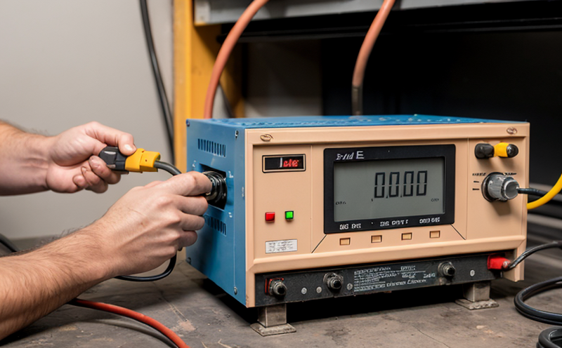
Die-level AVS testing focuses on individual semiconductor dies, which are the smallest functional units within a microchip. These tests can be performed using specialized equipment capable of applying controlled electrical stresses and monitoring the performance characteristics of each die under various stress conditions. The primary goal is to assess how well a die withstands high-voltage stress without failing.
The IEC 60749-71 standard provides detailed guidelines for the implementation of AVS testing, including the selection of appropriate test parameters such as voltage levels, temperature conditions, and duration of exposure. These parameters are crucial in accurately simulating real-world operational stresses that a semiconductor might encounter during its lifecycle.
During the testing process, each die is subjected to controlled stress until it either fails or meets predefined criteria for successful performance. The results from these tests are meticulously recorded and analyzed to provide insights into the reliability of the tested semiconductors. This information is invaluable for quality control, design optimization, and ensuring compliance with international standards.
The significance of IEC 60749-71 AVS testing extends beyond mere compliance; it plays a pivotal role in advancing semiconductor technology by identifying robust designs that can withstand harsh environments. By adhering to this standard, manufacturers can enhance product quality, reduce warranty costs, and improve overall customer satisfaction.
In summary, IEC 60749-71 AVS testing is an indispensable tool for ensuring the reliability of semiconductors at the die level. Its application in semiconductor manufacturing processes helps in identifying potential issues early on, thereby contributing to higher-quality products and more reliable electronic systems.
Environmental and Sustainability Contributions
The implementation of IEC 60749-71 AVS testing contributes significantly to environmental sustainability by promoting the development of robust semiconductor technologies. By ensuring that semiconductors can operate reliably under extreme conditions, this standard helps reduce the need for frequent replacements due to premature failures. This leads to extended product lifecycles and decreased waste generation.
Furthermore, IEC 60749-71 AVS testing supports sustainable practices by encouraging the design of semiconductors that are not only reliable but also energy-efficient. The ability to withstand high voltage stress without failure ensures that devices can operate efficiently under varying environmental conditions, reducing the overall power consumption and heat generation.
The standard's focus on durability also fosters a circular economy approach in electronics manufacturing by promoting longer product lifecycles and reduced electronic waste. By identifying weak points early in the development process, manufacturers can design more resilient components that are less prone to failure, thus extending the operational life of end products.
Overall, IEC 60749-71 AVS testing aligns with broader sustainability goals by enhancing product reliability and promoting efficient resource use. Its role in semiconductor manufacturing is crucial for building a more sustainable future in electronics technology.
Competitive Advantage and Market Impact
The adoption of IEC 60749-71 AVS testing can provide significant competitive advantages to companies operating within the semiconductor sector. By ensuring that their products meet stringent reliability standards, manufacturers can differentiate themselves in a crowded market. This not only enhances brand reputation but also attracts customers seeking high-quality and durable products.
Compliance with this standard demonstrates a commitment to excellence and quality assurance, which are key factors influencing customer trust and loyalty. Companies that lead the industry in adhering to such rigorous testing protocols can expect to see increased market share as they cater to growing demand for reliable semiconductor technologies.
The ability to consistently meet or exceed IEC 60749-71 AVS test requirements also opens up new opportunities for collaboration and partnerships with leading global players. These collaborations can facilitate knowledge sharing, technology transfer, and joint innovation efforts, further solidifying market positions.
Moreover, the standard's emphasis on environmental sustainability aligns with broader industry trends towards greener technologies. This alignment enhances a company’s image as an environmentally conscious entity, appealing to eco-conscious consumers who are increasingly prioritizing sustainable practices.
In conclusion, embracing IEC 60749-71 AVS testing is not just about meeting regulatory requirements but also about gaining strategic advantages that can drive business growth and market leadership.
Use Cases and Application Examples
The application of IEC 60749-71 AVS testing is extensive, covering various use cases in the semiconductor industry. One key area where this standard is applied is in the development of automotive semiconductors. These components must operate reliably under extreme temperatures and pressures found in vehicular environments.
Another critical application involves industrial electronics that are subjected to harsh environmental conditions such as high humidity, corrosive atmospheres, and mechanical shocks. By undergoing IEC 60749-71 AVS testing, these devices can be ensured of maintaining their operational integrity even under challenging circumstances.
In the consumer electronics sector, manufacturers use this standard to ensure that portable devices like smartphones and tablets can withstand voltage spikes without compromising performance or safety. This is particularly important given the increasing complexity and power demands of modern consumer electronics.
Additionally, IEC 60749-71 AVS testing is employed in the aerospace industry where reliability under extreme conditions is paramount. Aerospace semiconductors must endure rigorous testing to meet the stringent requirements set by regulatory bodies like NASA or ESA.
The telecommunications sector also benefits greatly from this standard as it helps ensure that network infrastructure components can function reliably even in remote and challenging locations.
By leveraging IEC 60749-71 AVS testing, these industries not only enhance the reliability of their products but also contribute to a safer and more efficient technological landscape. The application examples highlight how this standard plays a vital role across diverse sectors within the semiconductor industry.


