ASTM F1388 Die Oxide Thickness Electrical Measurement Testing
The ASTM F1388 standard provides a comprehensive approach to measuring die oxide thickness using electrical resistance methods. This service is essential for semiconductor and microchip manufacturers who need to ensure the quality, reliability, and performance of their products during various stages of production.
Die oxide thickness plays a critical role in the functionality and durability of semiconductors. The oxide layer acts as an insulator between the silicon substrate and the metal contacts, preventing short circuits and ensuring proper electrical isolation. ASTM F1388 is particularly useful for assessing the quality of this oxide layer during die-level testing.
The testing process involves measuring the electrical resistance of a thin oxide film on the surface of a semiconductor die using an alternating current (AC). The thickness of the oxide layer can be calculated based on the measured resistance. This method ensures that the oxide layer meets the specified thickness requirements, which are critical for the overall performance and reliability of the chip.
Preparation of samples is crucial before conducting ASTM F1388 tests. Each die must be carefully prepared to ensure accurate measurements. The surface should be clean and free from contaminants or residues that could affect the test results. Once prepared, the die is placed in a special fixture designed for electrical resistance measurement.
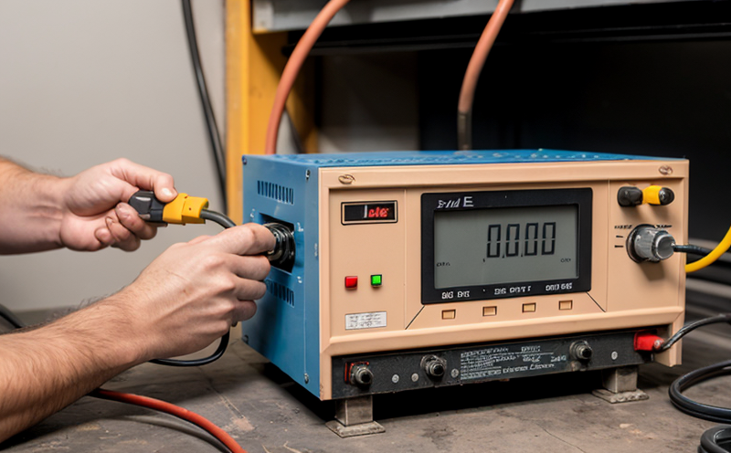
The testing equipment used for ASTM F1388 includes specialized fixtures, high-precision AC voltage sources, and data acquisition systems capable of recording detailed resistance measurements. The setup ensures consistent and repeatable results, which are essential for quality control processes.
ASTM F1388 specifies the acceptance criteria based on the expected oxide thickness values. These values are determined by industry standards and customer specifications. Compliance with these criteria is critical to ensure that the die meets the required performance levels. Non-compliance may lead to issues such as electrical shorts or poor insulation, affecting the overall reliability of the semiconductor.
By adhering strictly to ASTM F1388 guidelines, laboratories can provide reliable and accurate measurements of die oxide thickness, contributing significantly to the quality assurance processes in the semiconductor industry. This service is particularly valuable for manufacturers looking to maintain high standards in their production processes.
| Sample Preparation | Testing Equipment | Acceptance Criteria |
|---|---|---|
| Clean surface free from contaminants | Specialized fixtures and AC voltage sources | Compliance with industry standards and customer specifications |
| Consistent sample positioning for repeatable results | Data acquisition systems for accurate measurements | Absence of electrical shorts or poor insulation |
The ASTM F1388 method is widely used in the semiconductor industry due to its reliability and accuracy. It provides a standardized approach that ensures consistent results across different laboratories. This service is particularly beneficial for quality managers, compliance officers, R&D engineers, and procurement teams who need to ensure that their products meet stringent quality standards.
By leveraging ASTM F1388 die oxide thickness electrical measurement testing, manufacturers can enhance the reliability of their semiconductors, leading to improved product performance and customer satisfaction. This service plays a vital role in the development and production of high-quality semiconductor devices.
Benefits
The ASTM F1388 die oxide thickness electrical measurement testing offers numerous benefits for manufacturers in the semiconductor industry. By using this method, companies can ensure that their products meet stringent quality standards and performance requirements. This service provides several advantages:
- Improved Quality Control: The ASTM F1388 method allows for precise measurements of die oxide thickness, ensuring that each product meets the required specifications.
- Enhanced Reliability: By adhering to this standard, manufacturers can reduce the likelihood of electrical shorts and poor insulation, which are common issues in semiconductors.
- Cost Savings: Early detection of defects through ASTM F1388 testing helps prevent costly rework or scrap during production.
- Compliance with Industry Standards: The ASTM F1388 method ensures that products meet the latest industry standards, providing a competitive edge in the market.
In summary, the ASTM F1388 die oxide thickness electrical measurement testing is an essential service for manufacturers looking to enhance the quality and reliability of their semiconductors. This method provides precise measurements, reduces defects, ensures compliance with industry standards, and ultimately leads to cost savings and improved product performance.
Industry Applications
| Application | Description |
|---|---|
| Wafer Fabrication: | This method is used to measure oxide thickness during the wafer fabrication process, ensuring that each die meets the required specifications. |
| Die-Level Testing: | The ASTM F1388 method is applied at the die level to assess the quality of the oxide layer before packaging and assembly. |
| Package Assembly: | This service is used during package assembly to verify that the oxide thickness meets the required standards, ensuring proper electrical performance. |
| Quality Assurance: | The ASTM F1388 method is an integral part of quality assurance processes in semiconductor manufacturing, providing precise measurements and ensuring product reliability. |
The ASTM F1388 die oxide thickness electrical measurement testing has wide-ranging applications across the semiconductor industry. This service ensures that each step of the production process meets the required standards, leading to high-quality products with enhanced performance and reliability.
Environmental and Sustainability Contributions
- Energy Efficiency: By ensuring the quality of oxide layers in semiconductors, this testing method contributes to more efficient electronic devices, reducing overall energy consumption.
- Material Optimization: Precise measurements through ASTM F1388 help manufacturers optimize material usage, leading to reduced waste and lower environmental impact.
- Reduced Defects: Early detection of defects through this testing method reduces the need for rework or scrap, minimizing resource consumption and waste generation.
The ASTM F1388 die oxide thickness electrical measurement testing is not only beneficial for semiconductor manufacturers but also contributes to environmental sustainability. By ensuring high-quality products with optimized material usage and reduced defects, this service plays a crucial role in promoting sustainable practices within the industry.


