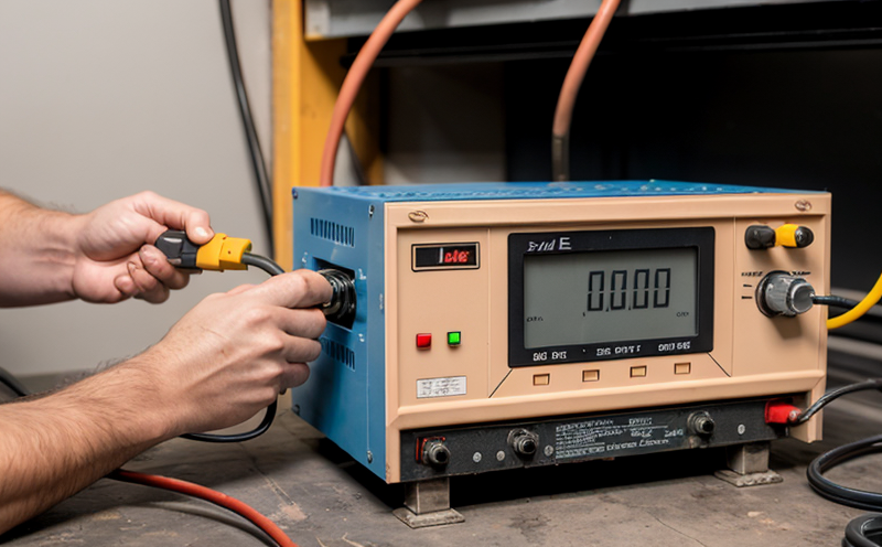
ASTM F1396 Die Defect Localization Electrical Testing
In semiconductor and microchip manufacturing, quality assurance is paramount. The ASTM F1396 Die Defect Localization Electrical Testing method provides a critical means to identify and localize defects at the die level before wafer-level assembly or package integration. This testing ensures that only defect-free dies are used in subsequent processes, thereby enhancing product reliability and reducing manufacturing costs.
The ASTM F1396 standard outlines procedures for performing electrical tests on individual dies within a semiconductor wafer to detect and quantify defects. Defects can include open circuits, shorts, and other issues that impact the functionality of the die. By using this method early in the manufacturing process, manufacturers can minimize the risk of incorporating defective dies into final products.
The test involves applying controlled electrical stimuli to each die while monitoring current flow or voltage changes. The data collected helps determine whether a die meets specified performance criteria. This approach is particularly useful for identifying subtle defects that might otherwise go undetected through visual inspection alone.
One of the key advantages of ASTM F1396 testing lies in its ability to provide precise localization of defects within individual dies. This capability allows manufacturers to isolate problematic areas and make informed decisions about whether to repair or discard specific dies, optimizing production efficiency and reducing waste.
The standard also emphasizes the importance of maintaining consistent test conditions across all samples being evaluated. Factors such as temperature, humidity, and voltage levels must be controlled rigorously to ensure accurate results. Compliance with these standards ensures that tests are repeatable and reliable, which is essential for quality assurance processes in semiconductor manufacturing.
For R&D engineers and quality managers, ASTM F1396 offers a robust framework for ensuring the integrity of their products. By incorporating this method into their testing protocols, they can ensure compliance with international standards while also enhancing product reliability and reducing costs associated with rework or scrapped components.
- Consistent Test Conditions: Maintaining stable environmental factors ensures accurate defect localization.
- Data Accuracy: Precise electrical measurements enable reliable identification of defects.
- Cost Efficiency: Early detection and resolution of issues save resources by minimizing rework or scrapping.
In summary, ASTM F1396 Die Defect Localization Electrical Testing plays a vital role in ensuring the quality and reliability of semiconductor products. It enables manufacturers to identify and address defects at an early stage, optimizing production processes and enhancing overall product performance.
Quality and Reliability Assurance
The ASTM F1396 Die Defect Localization Electrical Testing method is integral to the broader quality assurance efforts within semiconductor manufacturing. Ensuring that each die meets stringent electrical performance criteria not only enhances the reliability of end products but also contributes significantly to maintaining customer trust.
By implementing ASTM F1396, manufacturers can achieve several objectives:
- Precision Defect Localization: The method allows for accurate identification and localization of defects within individual dies. This precision is crucial in minimizing the impact of defective components on overall product performance.
- Data-Driven Decision Making: Comprehensive data collection provides insights into the quality of each die, enabling informed decisions about which dies to incorporate into final products.
- Cost Efficiency: Early identification and resolution of defects reduce waste and rework costs, leading to more efficient manufacturing processes.
The ASTM F1396 standard is designed to align with international quality assurance practices. By adhering to these standards, semiconductor manufacturers can ensure consistent product quality across their operations. This alignment also facilitates easier compliance with regulatory requirements, further enhancing the reputation and market standing of compliant organizations.
For procurement teams, ensuring adherence to ASTM F1396 helps maintain high standards throughout the supply chain. By selecting suppliers who employ this testing method, companies can guarantee that only defect-free dies are used in their products. This commitment to quality contributes to building long-term relationships with reliable partners and enhances overall product reliability.
In conclusion, ASTM F1396 Die Defect Localization Electrical Testing is a cornerstone of modern semiconductor manufacturing practices. Its focus on precision, data accuracy, and cost efficiency makes it an indispensable tool for maintaining high-quality standards in this critical industry sector.
Competitive Advantage and Market Impact
The implementation of ASTM F1396 Die Defect Localization Electrical Testing provides semiconductor manufacturers with a competitive edge by enhancing their ability to produce high-quality products consistently. This method ensures that only defect-free dies are used in final products, thereby improving reliability and customer satisfaction.
- Increased Market Share: By providing reliable and consistent product quality, companies can attract more customers and increase market share.
- Better Customer Trust: Ensuring high-quality products through rigorous testing builds trust with customers, fostering long-term relationships.
- Innovation Support: The ability to identify and resolve defects early in the manufacturing process supports continuous improvement efforts and fosters innovation within the organization.
The use of ASTM F1396 also positions companies as leaders in compliance with international standards, which is increasingly important in today's global market. By adhering to these standards, manufacturers can demonstrate their commitment to quality and reliability, further enhancing their reputation and market standing.
In conclusion, the adoption of ASTM F1396 Die Defect Localization Electrical Testing offers significant benefits for semiconductor manufacturers. It not only enhances product quality but also provides a strong competitive advantage in an increasingly demanding market environment.
Use Cases and Application Examples
The ASTM F1396 Die Defect Localization Electrical Testing method finds application across various sectors where high reliability is critical. One prominent example is the automotive industry, where microcontrollers play a crucial role in ensuring safe and efficient vehicle operations.
- Automotive Electronics: Ensuring the integrity of microcontrollers through ASTM F1396 testing helps enhance overall vehicle safety and performance.
- Aerospace & Defense: In this highly regulated sector, maintaining product reliability is essential. ASTM F1396 provides a standardized approach to ensure consistent quality in critical components.
- Consumer Electronics: For consumer devices like smartphones and tablets, the need for high-quality microprocessors cannot be overstated. This testing method helps maintain performance standards expected by consumers.
In addition to these sectors, semiconductor manufacturers across industries benefit from ASTM F1396 by ensuring that their products meet strict quality criteria. By integrating this testing into their manufacturing processes, companies can demonstrate their commitment to excellence and reliability, further solidifying their position in the competitive market landscape.
The versatility of ASTM F1396 makes it applicable across diverse applications within various industries. Its role in enhancing product reliability and ensuring compliance with international standards underscores its significance in modern semiconductor manufacturing practices.


