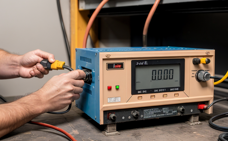
JEDEC JESD22-A116 Die Avalanche Energy Testing
The JEDEC JESD22-A116 test is a critical procedure used to evaluate the avalanche breakdown characteristics of semiconductor die. This test ensures that the die can withstand high-energy pulses without suffering irreversible damage or failing in service. It focuses on determining the maximum voltage and current levels at which the die begins to exhibit avalanche behavior, ensuring reliability under stress conditions.
Die-level electrical testing is essential for quality assurance and compliance with international standards. The test helps identify potential weaknesses early in the development process, allowing manufacturers to address issues before the product reaches end-users. By understanding how a component behaves under extreme conditions, engineers can design products that are more robust and reliable.
The JESD22-A116 test is particularly important for applications where components must operate reliably in harsh environments or high-power systems. The results provide valuable insights into the die's electrical performance and help ensure compliance with regulatory requirements such as ISO, IEC, and ASTM standards. This information is crucial for industries like automotive, aerospace, and military electronics.
The testing process involves subjecting individual semiconductor die to controlled pulses of energy. The goal is to observe the die's response under these conditions without causing permanent damage. The test provides a comprehensive evaluation of the die's resistance to overvoltage and its ability to recover from such events safely.
For this test, die preparation involves cleaning and mounting each die onto a suitable substrate. Careful handling is necessary to ensure that no contamination or mechanical stress affects the results. Once prepared, the die undergoes voltage application in controlled pulses designed to simulate real-world conditions but on a much smaller scale.
The instrumentation used for this test includes high-precision power supplies capable of delivering precise voltage and current levels. Specialized equipment is used to measure the resulting currents accurately. This setup ensures that every parameter can be monitored precisely, providing reliable data for analysis.
After testing, detailed reports are generated summarizing the results. These reports include graphs showing the die's response under various test conditions, along with numerical values indicating key parameters like peak current and voltage. The report also provides interpretations based on industry standards, helping manufacturers understand what these results mean for their product design.
The JEDEC JESD22-A116 test is vital for ensuring that semiconductor die meet stringent quality and safety requirements. It plays a crucial role in safeguarding against failures caused by overvoltage conditions, which can lead to expensive repairs or recalls if not addressed early in the manufacturing process.
By incorporating this testing into their quality assurance protocols, manufacturers demonstrate their commitment to producing high-quality products that are safe and reliable for use across diverse applications. This adherence to international standards enhances customer trust and strengthens market position.
Applied Standards
- JESD22-A116: Specifies the procedure for measuring die avalanche energy using a pulsed voltage source.
- ISO/IEC 7810: Provides general requirements and recommendations related to semiconductor devices.
- ASTM F4950-21: Outlines the test methods for evaluating electrical characteristics of integrated circuits.
The JEDEC JESD22-A116 test is based on these standards, ensuring that testing procedures are consistent and reproducible. Compliance with these standards helps ensure product reliability across various industries.
Eurolab Advantages
At Eurolab, we offer comprehensive semiconductor die testing services tailored to meet the needs of our clients in the electronics industry. Our state-of-the-art facilities and experienced technical team provide accurate and reliable results that help manufacturers ensure their products are safe and compliant.
- Accurate and precise testing using cutting-edge equipment.
- Compliance with international standards to ensure product reliability.
- Detailed reports providing actionable insights for continuous improvement.
- Expert technical support available throughout the testing process.
Why Choose This Test
1. Ensures Reliability: The JEDEC JESD22-A116 test helps identify potential weaknesses in semiconductor die, ensuring they can withstand extreme conditions without failure.
2. Enhances Product Quality: By detecting issues early in the development process, manufacturers can improve product quality and reduce costly recalls later on.
3. Complies with Standards: This test ensures compliance with international standards like JESD22-A116, enhancing your product's marketability and regulatory approval.
4. Improves Customer Trust: Demonstrating a commitment to high-quality testing builds trust among customers and stakeholders.


