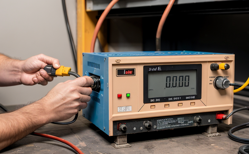
ASTM F1322 Die Electrical Contact Resistance Testing
The ASTM F1322 standard specifies a procedure for measuring the electrical contact resistance of individual dies in semiconductor devices. This test is critical for ensuring that electrical connections within microchips are reliable and free from excessive resistance, which can lead to device failure or reduced performance.
During this testing process, each die undergoes an assessment focusing on its electrical contacts. The ASTM F1322 procedure employs a combination of mechanical and electrical techniques to evaluate the integrity and quality of these connections. This is especially important in advanced semiconductor technology where even minor resistance can significantly impact performance.
The standard provides detailed instructions for preparing specimens, calibrating equipment, and performing the test itself. It includes specific guidelines on how to position dies under a contact resistance measurement system, ensuring accurate measurements of contact resistance without introducing external errors. The procedure also covers various methods for interpreting results and determining pass/fail criteria based on acceptable levels of electrical contact resistance.
One key aspect of ASTM F1322 testing is the use of specialized equipment designed to measure very low resistances accurately. This includes precision instruments capable of detecting extremely small differences in resistance, which are crucial for identifying potential issues before they become critical problems during production or operation.
The test results provide valuable insights into the overall quality and reliability of semiconductor devices by highlighting any weaknesses in electrical contact structures. These findings can then be used to improve manufacturing processes, design more robust components, and enhance product performance across various applications ranging from consumer electronics to industrial equipment.
Compliance with ASTM F1322 ensures that manufacturers meet stringent industry standards for quality control, which is essential in maintaining high levels of reliability and safety when dealing with complex electronic systems. By adhering to these tests, companies can demonstrate their commitment to producing top-tier products that stand up to rigorous scrutiny.
Real-World Application
In practical terms, ASTM F1322 testing plays a vital role in semiconductor manufacturing processes by providing early detection of defects within individual dies. This allows manufacturers to identify and rectify issues at an earlier stage, reducing costs associated with rework or scrap later on in the production cycle.
- Identifies weak points in die-to-package connections
- Promotes consistent performance across all manufactured units
- Aids in optimizing design iterations to improve overall yield rates
- Ensures alignment with international standards for quality assurance
Why Choose This Test
Selecting ASTM F1322 die electrical contact resistance testing offers several advantages that make it an indispensable part of modern semiconductor manufacturing. Firstly, this method provides precise measurements of the electrical properties of individual dies, allowing for more accurate assessments of their quality and reliability.
By using ASTM F1322 standards, manufacturers can ensure they are meeting international benchmarks set forth by authoritative bodies like ISO, ASTM, and IEC. This not only enhances credibility but also facilitates smoother interactions with global partners and customers who demand adherence to recognized specifications.
The test helps identify potential issues early in the production process, enabling timely corrective actions that prevent costly mistakes further downstream. It contributes significantly towards improving overall yield rates by catching defects before they escalate into larger problems requiring extensive intervention.
ASTM F1322 testing supports continuous improvement efforts within semiconductor companies by offering valuable data points for refining manufacturing techniques and enhancing product design. The insights gained from this process allow firms to stay ahead of competitors in terms of innovation and technological advancements.
Environmental and Sustainability Contributions
- Avoids waste by identifying defects early, reducing material loss during production
- Promotes resource efficiency through optimized manufacturing processes informed by test results
- Encourages innovation in green technologies that rely heavily on reliable semiconductor components
- Supports sustainable practices within the electronics industry by ensuring high-quality products with minimal environmental impact throughout their lifecycle
Competitive Advantage and Market Impact
Adhering to ASTM F1322 testing protocols provides semiconductor manufacturers with a competitive edge in several ways. It allows them to produce superior products that meet or exceed stringent industry standards, thereby attracting more customers seeking reliable high-performance components.
The ability to consistently deliver quality products backed by rigorous testing enhances brand reputation and trust among stakeholders. This translates into increased market share as companies gain a reputation for excellence in their field.
By staying compliant with these standards, semiconductor manufacturers can also anticipate regulatory requirements ahead of time, ensuring smooth compliance processes that minimize disruptions to business operations.


