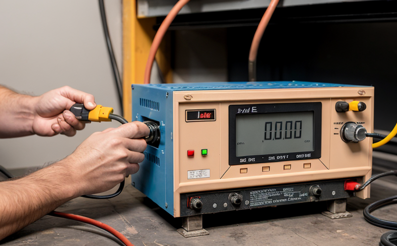
ASTM F1241 Die Dielectric Property Electrical Testing
The ASTM F1241 standard provides a comprehensive framework for dielectric property electrical testing at the die level. This method is essential in ensuring the reliability and performance of microchips and semiconductors, which are critical components in modern electronics. The test aims to assess the insulating properties of the dielectric materials used within semiconductor devices.
The ASTM F1241 procedure involves subjecting a die to various voltage levels while monitoring current flow. This allows for the determination of key electrical parameters such as capacitance, dissipation factor (tan delta), and insulation resistance. These metrics are crucial in identifying potential weaknesses or defects that could lead to device failure under operational conditions.
The testing process begins with thorough preparation of the die sample. Prior to testing, it is cleaned meticulously using appropriate solvents to remove any contaminants that might interfere with accurate measurements. The die is then mounted onto a suitable holder designed for electrical connections and mechanical stability during testing.
Once prepared, the die undergoes a series of voltage stress tests at progressively higher levels up to its rated maximum value. Simultaneously, current readings are recorded to compute relevant electrical parameters. This step-by-step approach ensures precise measurement of the dielectric properties across different stress conditions.
The ASTM F1241 methodology also includes post-test inspections aimed at identifying any visible changes indicative of material degradation or structural damage due to the applied stresses. Such observations provide additional insights into the robustness and longevity of the tested semiconductors.
Compliance with this standard is vital for quality control in semiconductor manufacturing, ensuring that products meet stringent industry standards before reaching marketplaces. By adhering strictly to ASTM F1241 guidelines, manufacturers can enhance product reliability and consumer trust.
The results from ASTM F1241 testing are typically reported comprehensively including dielectric constants, loss factors, breakdown voltages, and leakage currents. These data points serve as critical inputs for further R&D efforts aimed at improving semiconductor design and fabrication processes.
Industry Applications
| Application | Description |
|---|---|
| Quality Control in Semiconductor Manufacturing | Ensures adherence to strict quality standards and enhances product reliability. |
| R&D for New Semiconductor Designs | Provides valuable insights into material performance under various stress conditions. |
| Development of High-Power Devices | Helps in optimizing designs for better insulation properties and increased efficiency. |
| Compliance Testing | Aids in meeting regulatory requirements set by governing bodies worldwide. |
| Failure Analysis | Assists in identifying root causes of failures to improve future product iterations. |
| Supplier Evaluation | Sets benchmarks for evaluating suppliers based on consistent quality assurance practices. |
| New Product Introduction (NPI) | Supports the launch of new products by validating their compliance with industry norms. |
| Manufacturing Process Optimization | Enables continuous improvement in production techniques through detailed analysis. |
Environmental and Sustainability Contributions
The ASTM F1241 dielectric property electrical testing plays a pivotal role in enhancing environmental sustainability by promoting the development of more reliable and efficient semiconductor devices. By ensuring that each component meets rigorous quality standards, this test helps extend product lifecycles, reducing waste generation and overall resource consumption.
Furthermore, complying with ASTM F1241 fosters innovation towards greener manufacturing practices. Manufacturers can adopt sustainable materials and processes knowing they will pass stringent tests like those specified in the standard. This not only reduces environmental impact but also contributes positively to global sustainability goals.
The detailed insights gained from ASTM F1241 testing enable companies to design products that are not only robust against failure but also energy-efficient. Efficient semiconductors contribute significantly to reducing power consumption, thereby lowering greenhouse gas emissions associated with electricity generation.
By integrating these sustainable practices into their operations, businesses can demonstrate their commitment to environmental responsibility while maintaining competitive edge in the market. The ASTM F1241 standard thus serves as a cornerstone for both quality assurance and eco-friendly advancements within the semiconductor industry.
Use Cases and Application Examples
The ASTM F1241 dielectric property electrical testing is widely used in various applications across different sectors. In aerospace, for instance, ensuring that microchips can withstand extreme environmental conditions is paramount. By adhering to ASTM F1241 guidelines, manufacturers can guarantee that their components perform reliably even under harsh space environments.
In automotive electronics, the stringent testing requirements of ASTM F1241 help prevent malfunctions caused by electrical failures. This ensures safer driving experiences and reduces the risk of accidents due to unpredictable component behavior.
For consumer electronics manufacturers, compliance with this standard is crucial for maintaining high standards of safety and performance across diverse product lines. From smartphones to smart home devices, every electronic gadget must meet stringent quality benchmarks set forth by ASTM F1241.
The pharmaceutical industry also benefits from the rigorous testing protocols provided by ASTM F1241. Ensuring that medical equipment such as implantable devices operates flawlessly is critical for patient safety and effective treatment outcomes.


