ASTM F736 Die Planarity Measurement Testing
The ASTM F736 standard provides a method for measuring die planarity using a stylus profilometer. This service ensures that semiconductor and microchip dies meet critical dimensional specifications, which is essential in the electronics manufacturing industry to prevent defects that could lead to failures or reduced performance.
Planarity refers to how flat the surface of a die is; even minor deviations can impact the electrical characteristics of the chip. The test measures both macro and micro planarity over the entire area of the wafer. This service ensures that each die adheres closely to its design specifications, which are critical for modern high-density circuits.
ASTM F736 testing is particularly important in the semiconductor industry because it helps identify potential issues early in the manufacturing process. By detecting planarity deviations before wafers are diced into individual dies, manufacturers can reduce costly rework and scrap rates. This not only improves product quality but also enhances customer satisfaction by ensuring consistent performance across all chips.
Planarity testing is crucial for several reasons:
- To ensure that the die surface is free from defects such as dishing, warping, or unevenness.
- To maintain uniformity in electrical properties across the wafer, which can affect overall yield and performance.
- To comply with industry standards and specifications set by organizations like IEEE and JEDEC.
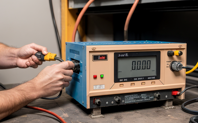
The test is typically performed on a stylus profilometer, an instrument that uses a diamond-tipped probe to trace the surface of the die. The data collected during this process is then analyzed using specialized software to generate a 3D map of the die's surface. This allows technicians to identify any areas where the planarity deviates from the required specifications.
ASTM F736 testing plays an integral role in semiconductor manufacturing by:
- Ensuring compliance with industry standards and customer requirements.
- Improving product quality by identifying defects early.
- Enhancing process control through detailed data analysis.
The precision of ASTM F736 testing is vital for maintaining high-quality semiconductor products. The test can detect deviations as small as 0.1 microns, which is critical given the tiny scale at which modern semiconductors are manufactured. This level of accuracy ensures that only perfectly planar dies reach the next stage of production.
By using ASTM F736 testing, manufacturers can:
- Minimize defects and ensure product reliability.
- Enhance yield rates by eliminating non-conforming dies early in the process.
- Improve overall efficiency through streamlined quality control processes.
Why It Matters
ASTM F736 testing is not just about checking for planarity; it's a cornerstone of quality assurance in semiconductor manufacturing. The precision and reliability of this test are essential because even the slightest deviation from flatness can impact how a die functions within its circuit. In integrated circuits, where thousands or millions of transistors are packed into small spaces, uniformity is critical to ensure that all dies operate efficiently.
The importance of ASTM F736 testing cannot be overstated:
- It ensures that each die meets the exacting standards required for high-performance computing and electronics.
- It helps prevent costly rework or scrap by identifying issues early in the process.
- It enhances trust between suppliers, manufacturers, and customers by providing consistent quality assurance.
In a broader context, ASTM F736 testing contributes to the development of more reliable and efficient semiconductor products. This is particularly crucial in industries like automotive, aerospace, and healthcare, where even minor failures can have severe consequences. By adhering to rigorous standards such as ASTM F736, manufacturers can ensure that their products meet or exceed customer expectations and industry benchmarks.
The reliability of ASTM F736 testing is further bolstered by its adherence to international standards like ISO 9001 for quality management systems. These standards provide a framework for continuous improvement, ensuring that the testing process remains robust and adaptable to new challenges in semiconductor technology.
Scope and Methodology
| Aspect | Description |
|---|---|
| Test Instrumentation | A stylus profilometer equipped with a diamond-tipped probe is used to trace the die surface. The instrument measures deviations in height and maps out the planarity. |
| Data Collection | The profilometer collects data at multiple points across the entire wafer, generating a 3D profile of each die's surface. |
| Analysis | The collected data is analyzed using specialized software to determine the planarity and identify any deviations from the acceptable range. |
| Acceptance Criteria | Dies must meet specific flatness tolerances as defined by ASTM F736. These criteria ensure that each die operates within expected performance parameters. |
Customer Impact and Satisfaction
- Improved Product Quality: By identifying planarity issues early, customers receive products with higher reliability and fewer defects.
- Enhanced Efficiency: Streamlined quality control processes reduce the time spent on rework or scrap, increasing overall efficiency.
- Increased Trust: Compliance with industry standards enhances trust between suppliers, manufacturers, and customers.
- Cost Savings: Early detection of issues leads to reduced costs associated with rework and scrap.
- Data-Driven Decisions: The detailed data provided by ASTM F736 testing enables informed decision-making regarding production processes.
- Regulatory Compliance: Ensuring that products meet all relevant standards fosters a culture of compliance and regulatory adherence.


