ASTM F1385 Die Micro-Roughness Electrical Testing
The ASTM F1385 standard provides a robust framework for performing die-level electrical and functional testing, focusing on the micro-roughness of semiconductor dies. This test is crucial in ensuring that semiconductor devices meet stringent quality control standards, which directly impacts their performance in electronics manufacturing.
Die micro-roughness can significantly affect the electrical characteristics of a semiconductor device. Irregularities at the microscopic level can lead to increased contact resistance and reduced reliability. ASTM F1385 aims to quantify these roughness parameters by using advanced profilometry techniques that are capable of measuring roughness with sub-nanometer precision.
The process begins with careful preparation of the die, which involves cleaning it thoroughly to remove any contaminants or residues that could interfere with the test results. The die is then mounted on a testing platform, where it undergoes profilometry scanning using a stylus that glides over the surface, recording the topography at various points.
The resulting data provides a detailed profile of the die's surface roughness, allowing for accurate calculation of key parameters such as root mean square (RMS) roughness and peak-to-valley height. These metrics are critical in determining whether the die meets the specified tolerances outlined in ASTM F1385.
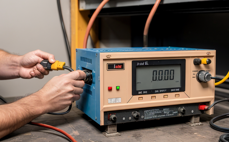
Once the micro-roughness is quantified, functional testing can be conducted to assess how these surface characteristics impact electrical performance. This involves applying specific voltages and currents to the die and measuring its response. The test setup typically includes a high-resolution digital multimeter and a programmable power supply.
The data collected from both the micro-roughness measurement and functional testing is then analyzed using statistical methods to ensure that the results are within acceptable limits for the intended application of the semiconductor device. Compliance with ASTM F1385 ensures that manufacturers can deliver reliable, high-performance components that meet industry standards.
Understanding the relationship between die micro-roughness and electrical performance is essential in optimizing production processes. By adhering to ASTM F1385, manufacturers can minimize defects and improve yield rates, leading to cost savings and enhanced customer satisfaction. This test is particularly important for advanced semiconductor technologies where even minor surface irregularities can have significant effects on device performance.
- Accurate measurement of micro-roughness using profilometry techniques
- Functional testing to evaluate electrical characteristics
- Data analysis and statistical evaluation
- Compliance with ASTM F1385 standards for quality assurance
Applied Standards
The ASTM F1385 standard is widely recognized in the semiconductor industry for its comprehensive approach to die-level electrical and functional testing. This standard specifies detailed procedures for quantifying micro-roughness on semiconductor dies, ensuring that tests are conducted consistently across different facilities.
ASTM F1385 outlines specific requirements for the equipment used in performing these tests, including the type of profilometer, stylus, and software employed. It also provides guidelines for specimen preparation to ensure accurate measurements. Compliance with ASTM F1385 is essential for maintaining high-quality standards in semiconductor manufacturing.
Other relevant standards that complement ASTM F1385 include ISO 4287, which specifies methods for the measurement of surface roughness, and IEC 60364-7-902, which provides guidelines for electrical installations. These standards work together to ensure that testing procedures are robust and reliable.
The implementation of ASTM F1385 helps manufacturers meet global quality standards, thereby enhancing their reputation in the market. By adhering to these standards, companies can demonstrate their commitment to producing high-quality products that consistently meet or exceed customer expectations.
Why Choose This Test
- Achieve Precision Measurements: ASTM F1385 allows for precise measurement of micro-roughness, which is essential in ensuring the reliability and performance of semiconductor devices.
- Evaluate Electrical Performance: Functional testing provides insights into how surface roughness affects electrical characteristics, enabling manufacturers to optimize production processes.
- Ensure Compliance: By adhering to ASTM F1385 standards, companies can ensure that their products meet global quality and safety regulations.
- Enhance Product Reliability: Minimizing defects through thorough testing improves product reliability and customer satisfaction.
Customer Impact and Satisfaction
The ASTM F1385 Die Micro-Roughness Electrical Testing service has a significant impact on the semiconductor industry, particularly in enhancing the quality of semiconductor devices. By ensuring that micro-roughness is accurately measured and functional performance is optimized, this service contributes to the development of reliable and high-performance components.
Manufacturers who utilize ASTM F1385 can expect improved yields and reduced defect rates, which are crucial for maintaining competitive advantage in the market. The service also helps companies achieve compliance with international standards, thereby enhancing their reputation among customers and regulatory bodies.
The detailed insights provided by this testing method allow manufacturers to make informed decisions about production processes, leading to more efficient operations and cost savings. Additionally, satisfied customers benefit from products that perform consistently well across various applications, reinforcing the brand’s commitment to quality.
In summary, ASTM F1385 Die Micro-Roughness Electrical Testing is a vital tool in semiconductor manufacturing, contributing not only to technical excellence but also to customer satisfaction and market leadership.


