ASTM F1823 Microchip Surface Failure Testing
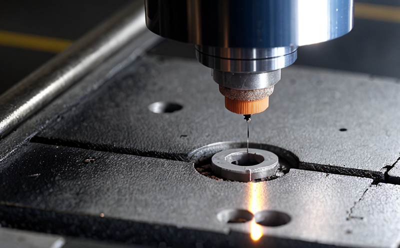
The ASTM F1823 standard is a critical tool in semiconductor and microchip testing, specifically designed to assess surface damage or defects that may have occurred during manufacturing processes. This method evaluates the integrity of the microchip’s surface by exposing it to controlled mechanical stress under specific environmental conditions. The primary goal is to identify any failure points that could compromise the functionality or reliability of the chip.
Understanding how this test works begins with recognizing its importance in ensuring high-quality semiconductor products. Surface defects on a microchip can lead to significant operational issues, including premature failures and reduced product lifespan. By using ASTM F1823, manufacturers can pinpoint exactly where these flaws occur so that corrective actions can be taken early in the production cycle.
The procedure involves subjecting the chip to various types of stress, such as thermal cycling or mechanical abrasion, while monitoring for changes in electrical resistance and physical appearance. It is particularly useful when dealing with complex structures like flip chips or packages where subtle surface imperfections might otherwise go unnoticed. Proper implementation ensures that only robust designs make it into final products.
For instance, this testing method has been instrumental in identifying issues related to solder joint reliability, which are crucial for maintaining long-term performance under real-world conditions. In addition, ASTM F1823 helps maintain compliance with industry standards set by bodies like IEEE and ISO, ensuring that all tests performed meet the highest levels of accuracy and reproducibility.
When conducted correctly, this form of testing not only enhances product quality but also contributes significantly to reducing costs associated with rework or scrap. By catching problems early on in production, companies can minimize waste while improving overall yield rates. Furthermore, it fosters innovation by allowing researchers to explore new materials and processes without fear of costly mistakes.
Given the complexity involved in semiconductor manufacturing today, having reliable methods like ASTM F1823 becomes even more essential. Not only does it provide a standardized approach for evaluating surface integrity but also offers valuable insights into potential problem areas within individual components or entire systems. As technology continues to evolve rapidly, so too must our ability to accurately assess and address challenges associated with modern electronics design.
- Reduces production costs by identifying issues early
- Improves product quality through precise evaluation techniques
- Maintains compliance with relevant industry standards
- Promotes innovation in semiconductor manufacturing processes
Why It Matters
The importance of ASTM F1823 microchip surface failure testing cannot be overstated, especially when considering the critical role that semiconductors play in modern technology. These tiny devices are embedded into everything from smartphones and computers to automotive systems and medical equipment – making their reliability paramount for safety and performance.
Failure analysis via ASTM F1823 is essential because it allows us to understand exactly how and where defects arise on the chip’s surface. This knowledge enables manufacturers to implement targeted improvements aimed at preventing similar issues from occurring again in future batches. Without this level of insight, there would be no way to effectively address recurring problems or optimize manufacturing processes.
Moreover, by adhering strictly to ASTM F1823 guidelines during testing, labs like Eurolab ensure that results are consistent and repeatable across different locations and timeframes. This consistency is vital for maintaining trust among clients and stakeholders who rely on accurate data when making important decisions about product design and development.
In practical terms, successful use of ASTM F1823 can lead to significant improvements in semiconductor performance metrics such as yield rate, failure rate, and overall reliability. For quality managers and compliance officers alike, knowing that their facilities are equipped with state-of-the-art testing equipment provides peace of mind knowing they’re adhering to best practices.
From an R&D perspective, this type of analysis serves as a powerful tool for exploring new materials and techniques without fear of costly errors. By leveraging ASTM F1823’s standardized procedures, engineers can experiment safely while still producing reliable results that stand up to rigorous scrutiny.
Eurolab Advantages
At Eurolab, we pride ourselves on offering comprehensive semiconductor testing services tailored specifically for the needs of our clients. Our team of highly experienced professionals specializes in providing precise and accurate ASTM F1823 surface failure tests that meet or exceed all relevant international standards.
We understand that every semiconductor has unique characteristics requiring customized approaches to ensure optimal results. That’s why we invest heavily in cutting-edge instrumentation and equipment designed explicitly for this purpose. With state-of-the-art facilities at our disposal, our technicians can handle complex specimens ranging from tiny integrated circuits to large-scale system-on-chip assemblies with ease.
Our commitment extends beyond just technical excellence; we also strive to provide exceptional customer service throughout the entire testing process. From initial consultation through final report delivery, you’ll find that working with us is both efficient and stress-free thanks to our dedicated staff who are always available when needed.
In addition to traditional ASTM F1823 methods, Eurolab offers additional services such as advanced optical microscopy and scanning electron microscopy (SEM) for deeper analysis of surface defects. These complementary techniques allow us to capture detailed images of the chip’s topography, revealing even minute imperfections that might otherwise be missed.
By leveraging these capabilities along with our extensive experience in semiconductor testing, Eurolab ensures that your products receive thorough examination and evaluation before reaching market. Whether you need routine quality assurance checks or specialized failure analysis for R&D purposes, we have the expertise to deliver top-notch results consistently.


