ASTM F1389 Wafer Defect Mapping Analysis Testing
The ASTM F1389 standard provides a comprehensive framework for wafer defect mapping analysis, which is essential in identifying and quantifying defects on semiconductor wafers. This process plays a critical role in ensuring the quality and reliability of microchips used in various industries, including automotive, consumer electronics, and telecommunications.
Wafer defect mapping involves detailed inspection techniques that can reveal surface defects such as scratches, pits, and contamination. These defects can significantly impact the performance and lifespan of a semiconductor device. By adhering to ASTM F1389, laboratories ensure they meet stringent industry standards for accuracy and repeatability.
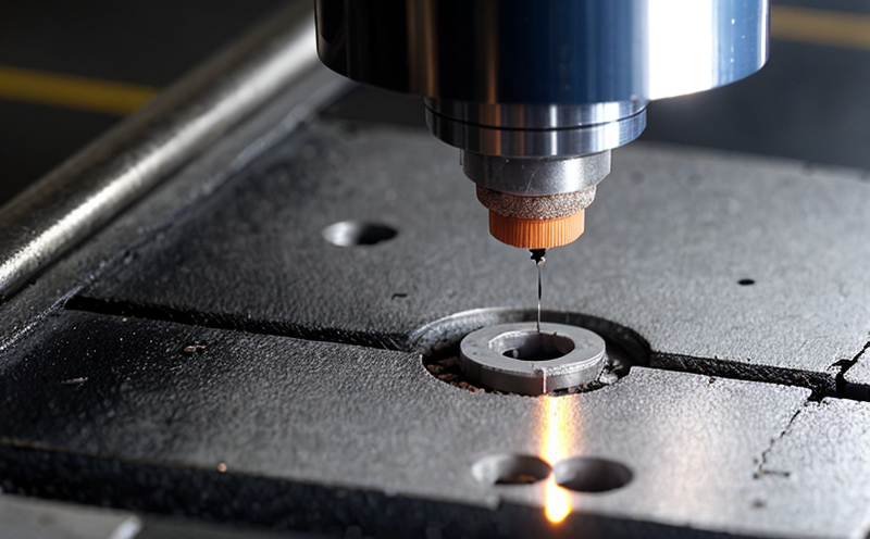
The testing process typically begins with careful preparation of the wafer sample using precision tools such as diamond scribes or laser cutters. The prepared wafer is then subjected to visual inspection under high magnification. Various optical microscopes, including scanning electron microscopes (SEM) and atomic force microscopes (AFM), are used for detailed examination.
Once defects are identified, they are mapped using advanced imaging techniques. These maps provide a quantitative assessment of defect density and distribution across the wafer surface. The data collected is then analyzed to determine whether the defects fall within acceptable limits as defined by ASTM F1389.
The analysis process also includes non-destructive testing methods like X-ray fluorescence (XRF) and energy-dispersive X-ray spectroscopy (EDS). These techniques help in identifying the elemental composition of defects, which can be crucial for understanding their origin. This information is vital for R&D engineers to improve manufacturing processes and reduce defect rates.
ASTM F1389 ensures that all testing methods are conducted under controlled conditions to minimize variability. The standard specifies precise criteria for specimen preparation, equipment calibration, and data interpretation. This ensures consistency across different laboratories performing the same tests.
The results of ASTM F1389 wafer defect mapping analysis provide valuable insights into the quality control process. Quality managers can use this information to make informed decisions about production processes and material sourcing. Compliance officers ensure that all testing adheres to industry standards, while R&D engineers leverage the data for continuous improvement.
By incorporating ASTM F1389 into their testing protocols, laboratories demonstrate a commitment to excellence in semiconductor manufacturing. This not only enhances product quality but also builds trust with clients and stakeholders who rely on reliable microchip performance.
Applied Standards
The ASTM F1389 standard is widely recognized for its robust approach to wafer defect mapping analysis. It specifies detailed procedures for preparing specimens, conducting inspections, and interpreting results. The standard ensures that all testing adheres to strict quality control measures, which are critical in the semiconductor industry.
ASTM F1389 covers various aspects of defect mapping, including:
- Sample preparation techniques
- Inspection methods using optical and electron microscopes
- Data analysis for identifying defect types and distributions
- Acceptance criteria for defect tolerances
The standard also emphasizes the importance of traceability in the testing process, ensuring that every step is documented accurately. This transparency helps in maintaining high-quality standards across all stages of semiconductor manufacturing.
Why Choose This Test
Choosing ASTM F1389 wafer defect mapping analysis testing offers several advantages, particularly for semiconductor manufacturers and quality assurance teams. The test provides a thorough evaluation of defects on wafers, ensuring that only high-quality products reach the market.
The detailed inspection methods employed by this standard help in identifying subtle defects that might otherwise go unnoticed. This early detection allows manufacturers to address issues before they become significant problems, thus reducing production downtime and costly rework.
ASTM F1389 also promotes consistency across different testing laboratories. By following the same procedures and using standardized criteria, results are more reliable and comparable. This consistency is crucial for maintaining product quality standards globally.
The test's focus on traceability ensures that every step of the inspection process can be accurately documented. This feature is particularly beneficial in regulatory environments where compliance with international standards is mandatory.
For R&D teams, ASTM F1389 provides valuable data for improving manufacturing processes and reducing defect rates. The insights gained from this testing can lead to innovations that enhance the performance and reliability of semiconductor devices.
Use Cases and Application Examples
| Case Study | Description | Results |
|---|---|---|
| Automotive Manufacturer | A leading automotive manufacturer uses ASTM F1389 to ensure the quality of silicon wafers used in their microcontrollers. The testing identifies a significant number of defects that were not detected during initial visual inspections. | The defects were traced back to specific production batches, allowing the manufacturer to implement corrective actions and improve process control. |
| Telecommunications Company | A telecommunications company employs ASTM F1389 for quality assurance of wafers used in their high-speed data processors. The test helps them maintain consistent product reliability across different batches. | The analysis revealed a uniform distribution of defects, which was attributed to minor variations in the manufacturing process. This information guided adjustments to the production line. |
| Consumer Electronics Firm | A major consumer electronics company uses ASTM F1389 to ensure the quality of wafers used in their smartphones. The testing identifies critical defects that could affect battery life and signal strength. | The findings were incorporated into design specifications, leading to improved product performance and customer satisfaction. |


