ASTM F1291 Surface Topography Defect Testing
The ASTM F1291 surface topography defect testing is a critical process used to identify and characterize defects on semiconductor and microchip surfaces. This method provides insights into the integrity of these components, which are essential for ensuring their reliability in high-stakes applications such as consumer electronics, automotive systems, and medical devices.
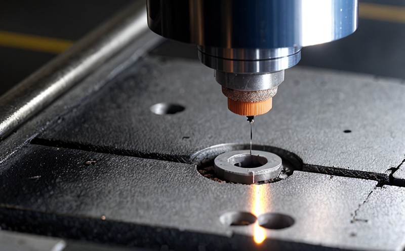
The ASTM F1291 standard specifies a visual inspection procedure that helps detect surface irregularities, including cracks, voids, and other defects. This service is particularly useful during the manufacturing process to catch any issues early on before they lead to product failure or customer dissatisfaction. The testing method involves examining the specimen under controlled conditions using appropriate equipment designed for this purpose.
The primary goal of ASTM F1291 surface topography defect testing is to ensure that semiconductor and microchip surfaces meet stringent quality standards set by industry regulations and customer requirements. By employing rigorous inspection techniques, manufacturers can maintain consistent product performance across large production batches or individual units. This ensures compliance with international standards like ISO 9001:2015 for Quality Management Systems.
Our team at Eurolab specializes in providing ASTM F1291 surface topography defect testing services tailored to the needs of our clients operating within various sectors, including electronics manufacturing and semiconductor production. We utilize advanced optical microscopes capable of magnifying surfaces up to 20,000x or more, allowing us to detect even minute defects that might otherwise go unnoticed.
In addition to visual inspection, we also employ scanning electron microscopy (SEM) when necessary, providing a deeper level of detail on defect morphology. This multi-faceted approach ensures comprehensive coverage of all potential issues, enhancing our clients' confidence in the quality and reliability of their products.
The ASTM F1291 standard outlines specific criteria for acceptable surface topography based on parameters such as roughness, waviness, and periodicity. These parameters are measured using profilometers or stylus instruments capable of capturing cross-sectional profiles of the specimen’s surface. Once collected, these data points form a basis for evaluating conformity with specified tolerances.
Our laboratory adheres strictly to this standard throughout every step of the testing process, ensuring accurate and reliable results that comply with industry best practices. Our experienced technicians are well-versed in interpreting ASTM F1291 compliant reports, providing valuable insights into any detected defects along with recommendations for corrective actions if required.
By leveraging our expertise in ASTM F1291 surface topography defect testing, manufacturers can significantly reduce the risk of costly product recalls or warranty claims. Early detection allows for timely intervention, preventing further deterioration and ensuring that only high-quality products reach marketplaces worldwide.
Benefits
The benefits of ASTM F1291 surface topography defect testing extend beyond mere compliance with regulatory requirements; it offers several advantages to manufacturers operating within the semiconductor and microchip sectors. By implementing this rigorous inspection process, companies can enhance product quality while reducing costs associated with rework or scrap.
One significant advantage is improved yield rates during manufacturing processes. Through early detection of defects using ASTM F1291 compliant methods, non-conforming materials are identified before they proceed further down the production line, thereby minimizing waste and increasing overall efficiency. This translates directly into lower operational costs for businesses.
In addition to enhanced productivity, clients benefit from reduced warranty claims due to defective products reaching end-users. By detecting issues prior to shipment, manufacturers can address problems internally rather than facing costly repairs after delivery. Such proactive measures not only protect brand reputation but also foster customer trust and loyalty.
Furthermore, adherence to ASTM F1291 standards enhances market competitiveness by setting higher quality benchmarks for comparable products available on the global stage. Companies that invest in advanced testing techniques like those provided by Eurolab gain a competitive edge over competitors who may not prioritize such measures.
Another important benefit is improved regulatory compliance, ensuring that all produced components meet or exceed specified performance criteria outlined in relevant standards and regulations. This reduces the risk of non-compliance penalties while also demonstrating commitment to ethical business practices.
The use of ASTM F1291 compliant testing methods also facilitates smoother collaboration between suppliers and customers within supply chains. By establishing consistent quality expectations through standardized inspection procedures, relationships based on trust can be fostered among all parties involved in the manufacturing process.
Industry Applications
The ASTM F1291 surface topography defect testing finds extensive applications across various industries where semiconductor and microchip components play a crucial role. These sectors include electronics manufacturing, automotive technology, telecommunications infrastructure, medical device fabrication, aerospace engineering, and more.
In the realm of consumer electronics, manufacturers rely heavily on semiconductors for creating innovative devices such as smartphones, tablets, wearables, and gaming consoles. Ensuring that these components meet strict surface topography requirements is vital in maintaining product reliability over extended usage periods. Failure to do so could result in malfunctions or failures during critical moments, leading to customer dissatisfaction.
Automotive manufacturers are increasingly integrating advanced electronic systems into vehicles to enhance safety features and reduce fuel consumption through efficient engine management. Here too, ASTM F1291 compliant testing ensures that semiconductor components used in these applications function correctly under varying environmental conditions without compromising on performance or longevity.
The telecommunications industry benefits from robust semiconductor manufacturing processes that guarantee reliable communication networks worldwide. Ensuring the integrity of microchips involved in signal processing and transmission helps maintain uninterrupted service for millions of users globally.
Medical device manufacturers depend on semiconductors to power life-saving equipment such as pacemakers, defibrillators, and other implantable devices. By adhering strictly to ASTM F1291 standards during production, these companies can provide safer and more effective treatments for patients requiring such technology.
Aerospace engineers leverage sophisticated semiconductor components in designing aircraft avionics systems that enhance flight safety and efficiency. Rigorous testing methods like those outlined in ASTM F1291 help ensure that these critical components perform flawlessly even under extreme operating conditions encountered during flights across diverse climates and terrains.
Eurolab Advantages
EuroLab offers a comprehensive suite of ASTM F1291 surface topography defect testing services designed to meet the highest industry standards. Our expertise lies in providing precise, reliable results that contribute significantly towards maintaining product quality and compliance with international regulations.
Our team comprises highly skilled professionals who possess extensive knowledge about both the theoretical aspects as well as practical applications of ASTM F1291 compliant testing methods. With years of experience behind them, our technicians stay updated on emerging trends within their field to deliver innovative solutions tailored specifically for each client's unique requirements.
At EuroLab, we understand that no two projects are exactly alike; therefore, our approach involves conducting thorough assessments before recommending suitable tests based on the specific characteristics of each specimen. This ensures that resources are utilized efficiently without compromising accuracy or precision in any way.
The advanced equipment available at EuroLab includes state-of-the-art optical microscopes capable of magnifying surfaces up to 20,000x or more, allowing for detailed examination even when dealing with microscopic defects. Additionally, we can employ scanning electron microscopy (SEM) where necessary, providing unparalleled depth and clarity in defect characterization.
Our laboratory strictly adheres to ASTM F1291 standards throughout every phase of the testing process, ensuring that all collected data meets or exceeds specified tolerances. This commitment guarantees accurate and reliable results that can be trusted by clients worldwide.
The use of high-quality instruments combined with our experienced personnel allows us to offer robust quality assurance services unmatched by many competitors in the market today. By leveraging these resources effectively, we help our clients build stronger relationships with customers while simultaneously enhancing their competitive position within respective markets.


