ASTM E3 Microstructural Preparation for Failure Analysis Testing
The ASTM E3 microstructural preparation method is a critical step in failure analysis and defect characterization. This process involves the careful preparation of a semiconductor or microchip specimen to ensure that any defects, cracks, or other anomalies can be accurately identified under microscopic examination. The goal is to provide a clear view of the material's internal structure so that engineers and quality managers can make informed decisions about the root cause of failure.
ASTM E3 is widely recognized in the semiconductor industry for its stringent requirements on specimen preparation, which are essential for accurate defect characterization. When performing this test, it is crucial to follow standardized procedures meticulously to avoid introducing artifacts or altering the true nature of the defects present in the sample.
The microstructural examination can reveal various types of failures including intergranular cracking, grain boundary segregation, and other microscopic issues that are not visible through macroscopic inspection. By using ASTM E3, laboratories ensure they meet industry standards for precision and repeatability, which is vital for quality assurance in the semiconductor sector.
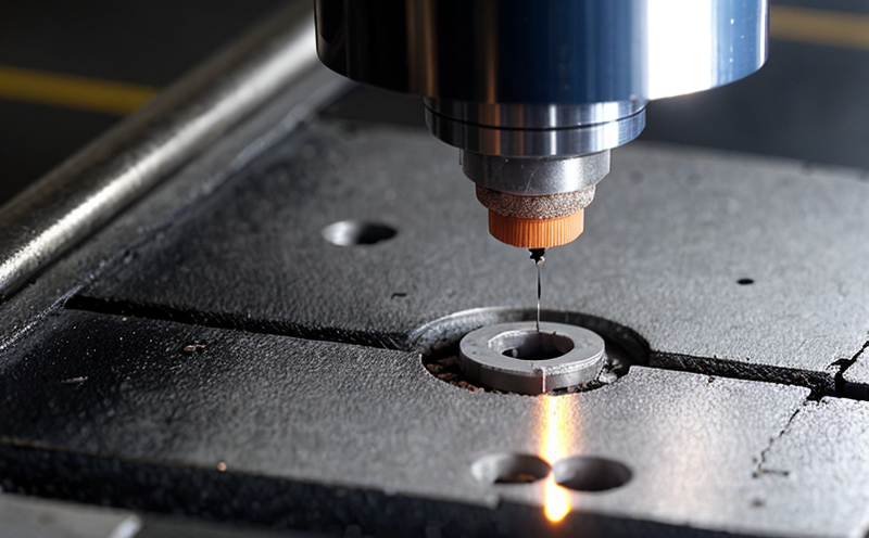
Failure analysis with ASTM E3 involves several steps: cleaning of the specimen to remove any contaminants or residues; precise cutting or grinding of the sample to obtain a representative cross-section; polishing to achieve a mirror-like finish suitable for microscopic examination; and finally, etching if necessary to enhance contrast between different material phases.
It is essential that all these stages are carried out under controlled conditions to prevent damage to the specimen. The cleanliness of tools used during preparation can significantly affect the outcome of the analysis. Therefore, only high-quality abrasives, solvents, and polishing compounds should be employed. Additionally, the choice of etchant plays a crucial role in revealing the microstructure accurately.
Once prepared, the sample is examined under a scanning electron microscope (SEM) or optical microscope depending on the required resolution. This detailed examination allows for precise identification of defects which can then be correlated back to manufacturing processes or operational conditions leading up to failure.
The importance of ASTM E3 cannot be overstated; it provides an objective basis upon which decisions regarding product design improvements, process changes, and regulatory compliance can be made confidently.
Understanding the specific requirements outlined in ASTM E3 helps ensure that specimens are prepared correctly for subsequent analysis. Compliance with these standards ensures reliable data collection and interpretation, thereby enhancing overall quality control practices within semiconductor manufacturing environments.
- Industry Applications: Semiconductor testing, failure analysis, defect identification, process optimization
Applied Standards
The ASTM E3 microstructural preparation method is based on several internationally recognized standards that provide guidance on specimen preparation for optical and scanning electron microscopy. These include:
- ASTM E1407-18: Standard Practice for Microstructural Examination of Metals, Alloys, and Intermetallics
- ASTM E3-19: Standard Terminology Relating to Metallic Materials
- ASTM E2305-17: Guide for Preparation of Semiconductor Device Samples for Scanning Electron Microscopy Examination
These standards outline the precise techniques and procedures necessary to prepare semiconductor samples accurately. They ensure consistency across different laboratories, facilitating accurate comparison of results.
The use of these standardized methods helps maintain high-quality testing practices throughout the industry. By adhering strictly to ASTM E3 guidelines, laboratories can produce reliable data that contribute significantly towards improving product quality and reducing failures in production processes.
Scope and Methodology
The scope of ASTM E3 microstructural preparation includes all aspects related to preparing semiconductor or microchip specimens for failure analysis using optical and scanning electron microscopy. The methodology involves several key steps:
- Cleaning: Removal of any contaminants from the specimen surface.
- Cutting: Precise cutting along a plane perpendicular to the grain direction to obtain a representative cross-section.
- Polishing: Grinding and polishing using progressively finer abrasives until a mirror-like finish is achieved.
- Etching (if necessary): Application of an etchant to enhance contrast between different material phases for better visibility under the microscope.
The entire process must be conducted in a cleanroom environment to minimize contamination risks. Each step requires careful control and precision, making it essential that experienced personnel perform this work.
After preparation, the specimen undergoes thorough inspection using advanced imaging techniques such as SEM or optical microscopy. This allows for detailed observation of the microstructure, enabling accurate identification of defects like cracks, voids, or inclusions. The findings from these examinations are used to inform corrective actions aimed at preventing similar issues in future productions.
Compliance with ASTM E3 ensures that labs adhere to best practices, ensuring accurate and reliable results. This not only enhances the credibility of test outcomes but also supports continuous improvement efforts within semiconductor manufacturing companies.


