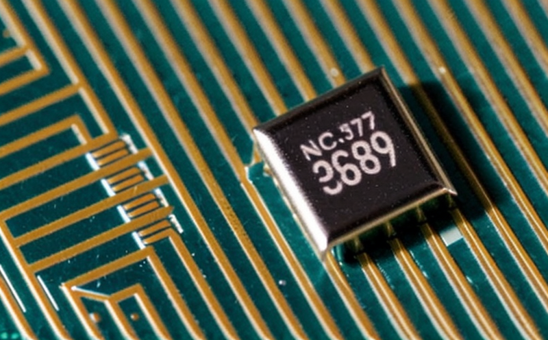
JEDEC JESD22-A145 Microchip Burn-in Stress Testing
The JEDEC JESD22-A145 test is a critical procedure used to enhance the reliability and lifetime of semiconductor devices, particularly in high-reliability applications. This stress test simulates real-world operating conditions that microchips might encounter during their operational life. By subjecting components to extended periods of operation at elevated temperatures and voltages, this burn-in process helps identify potential failures early on, ensuring only robust and reliable parts are deployed.
The JESD22-A145 test is particularly relevant for industries where the failure rate of microchips can be extremely high if not adequately screened. For instance, automotive electronics, aerospace components, and medical devices require microchips that can endure rigorous operating conditions without compromising performance or safety. The test helps manufacturers identify early-stage reliability issues such as latent defects, solder joint failures, and electrical overstress.
The process involves placing the microchips on a specialized burn-in board where they are subjected to elevated temperatures (up to 150°C) and voltages that exceed their rated values. The test typically lasts for several hours, depending on the specific requirements set by the manufacturer or regulatory bodies. This extended exposure helps in accelerating potential failures, allowing for early detection and removal of defective units.
The JEDEC JESD22-A145 test is not just a formality but a crucial step in ensuring that microchips meet stringent quality standards. It ensures that the devices can withstand the rigors of real-world use without degradation or failure. This testing is particularly important for high-reliability applications where downtime could be costly or dangerous.
For industries such as automotive, aerospace, and medical devices, the reliability of microchips cannot be overstated. The JESD22-A145 test helps in reducing field failures by identifying defects that might not become apparent under normal operating conditions. This proactive approach to quality control ensures that only reliable components are used in critical applications.
The process is meticulously controlled and monitored, with real-time data collection on parameters such as temperature, voltage, current, and power dissipation. This continuous monitoring allows for precise control over the test environment, ensuring accurate results that reflect the actual conditions the microchips will encounter in use. The testing also provides valuable insights into the thermal and electrical behavior of the components under stress.
After the burn-in process, the microchips are thoroughly inspected to identify any signs of failure or degradation. This step is crucial as it allows for the early detection of potential issues that could lead to field failures. The use of advanced inspection tools helps in identifying subtle defects that might not be apparent during initial testing.
The JESD22-A145 test is an essential part of the quality assurance process, ensuring that microchips meet or exceed industry standards and customer expectations. By incorporating this test into their production processes, manufacturers can significantly enhance the reliability and longevity of their products, thereby building trust with customers and stakeholders.
Industry Applications
- Aerospace: Ensures microchips used in avionics systems are robust enough to withstand extreme temperatures and vibrations.
- Automotive: Guarantees the reliability of control units that manage critical functions like braking, steering, and engine management.
- Medical Devices: Helps in verifying the safety and performance of microchips used in life-saving equipment such as pacemakers and defibrillators.
- Telecommunications: Ensures the reliability of network infrastructure components that handle high data throughput.
Why Choose This Test
The JEDEC JESD22-A145 burn-in stress test is a cornerstone in ensuring the robustness and reliability of semiconductor devices, particularly in high-reliability applications. Here are several reasons why this test is indispensable:
Firstly, it provides an early detection mechanism for latent defects that might not be apparent during initial testing. By subjecting microchips to extended periods of operation at elevated temperatures and voltages, the burn-in process helps in accelerating potential failures, allowing for their identification and removal before they impact the end product.
Secondly, this test ensures compliance with industry standards such as JESD22-A145, which are designed to protect consumers from potentially hazardous products. By adhering to these standards, manufacturers can ensure that their products meet the highest quality and safety benchmarks.
Thirdly, the JESD22-A145 test helps in reducing field failures by identifying defects early on. This proactive approach not only enhances product reliability but also minimizes the risk of costly recalls and warranty claims. By incorporating this test into their production processes, manufacturers can build a strong reputation for quality and customer satisfaction.
Finally, the burn-in process provides valuable insights into the thermal and electrical behavior of microchips under stress conditions. This data is crucial for optimizing design parameters and improving overall product performance. The use of advanced inspection tools during this test ensures that even subtle defects are identified, leading to more robust and reliable products.
In conclusion, the JEDEC JESD22-A145 burn-in stress test is an essential tool in ensuring the reliability and longevity of semiconductor devices. Its ability to identify latent defects early on, ensure compliance with industry standards, reduce field failures, and provide valuable design insights makes it an indispensable part of any quality assurance process.
Quality and Reliability Assurance
The JEDEC JESD22-A145 burn-in stress test plays a vital role in enhancing the reliability and longevity of semiconductor devices, particularly in high-reliability applications. By subjecting microchips to extended periods of operation at elevated temperatures and voltages, this test helps in accelerating potential failures, allowing for their early detection and removal.
The process is meticulously controlled and monitored, with real-time data collection on parameters such as temperature, voltage, current, and power dissipation. This continuous monitoring ensures accurate results that reflect the actual conditions the microchips will encounter in use. The testing also provides valuable insights into the thermal and electrical behavior of the components under stress.
After the burn-in process, the microchips are thoroughly inspected to identify any signs of failure or degradation. This step is crucial as it allows for the early detection of potential issues that could lead to field failures. The use of advanced inspection tools helps in identifying subtle defects that might not be apparent during initial testing.
The JESD22-A145 test is an essential part of the quality assurance process, ensuring that microchips meet or exceed industry standards and customer expectations. By incorporating this test into their production processes, manufacturers can significantly enhance the reliability and longevity of their products, thereby building trust with customers and stakeholders.
The use of advanced inspection tools during this test ensures that even subtle defects are identified, leading to more robust and reliable products. This proactive approach not only enhances product reliability but also minimizes the risk of costly recalls and warranty claims. By adhering to industry standards such as JESD22-A145, manufacturers can ensure that their products meet the highest quality and safety benchmarks.
In conclusion, the JEDEC JESD22-A145 burn-in stress test is an indispensable tool in ensuring the reliability and longevity of semiconductor devices. Its ability to identify latent defects early on, ensure compliance with industry standards, reduce field failures, and provide valuable design insights makes it an essential part of any quality assurance process.


