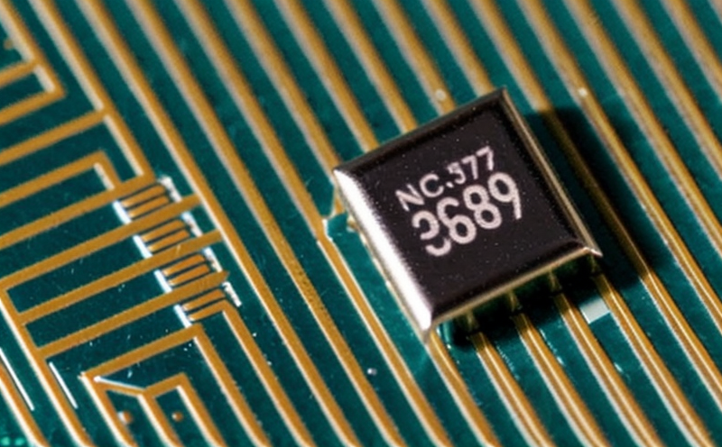
ASTM F1241 Dielectric Properties Reliability Testing
The ASTM F1241 standard is a critical tool in the semiconductor and microchip testing sector. It focuses on dielectric properties, which are fundamental to understanding how semiconductors behave under various environmental conditions. This test ensures that the reliability of semiconductors is maintained over their lifetime, making it indispensable for quality managers, compliance officers, R&D engineers, and procurement teams.
The ASTM F1241 standard evaluates dielectric properties by measuring capacitance and dissipation factor (tan δ) in a controlled environment. This process helps determine the stability of semiconductor devices under high-frequency conditions, which is essential for ensuring their performance over extended periods. The test is particularly important as it can predict potential failures due to environmental factors such as temperature changes, humidity, and voltage stress.
The reliability of semiconductors is not just about their initial performance but also how they hold up under real-world conditions. By using ASTM F1241, manufacturers can ensure that their products meet the stringent requirements set by industry standards and regulatory bodies. This ensures product longevity and customer satisfaction, which are crucial for maintaining a competitive edge in the market.
The methodology behind ASTM F1241 involves subjecting semiconductor samples to a series of tests designed to simulate real-world conditions. These tests include exposure to varying temperatures, humidity levels, and voltage stresses. The results provide insights into how well the semiconductors can withstand these environmental factors without degrading their dielectric properties.
The importance of ASTM F1241 cannot be overstated in today’s competitive market. It helps identify potential weaknesses early on, allowing for corrective actions to be taken before product launches. This proactive approach not only enhances the reliability of semiconductors but also reduces production costs associated with post-launch repairs and replacements.
Moreover, ASTM F1241 contributes significantly to environmental sustainability by promoting the development of longer-lasting products. By ensuring that semiconductors meet rigorous testing standards, companies can contribute positively to reducing electronic waste and minimizing resource consumption.
Why It Matters
The ASTM F1241 standard plays a pivotal role in semiconductor reliability by providing a standardized approach to evaluating dielectric properties. This is crucial because it ensures that all tests are conducted under controlled conditions, which minimizes variability and enhances the accuracy of results.
- Controlled Environment Testing: ASTM F1241 specifies the precise environmental conditions necessary for accurate testing. These include temperature ranges from -65°C to +150°C and humidity levels up to 98% RH. By maintaining these controlled environments, the standard ensures consistent results across different test cycles.
- Data Accuracy: The use of standardized methods enhances data accuracy, which is essential for making informed decisions about product design and manufacturing processes. Accurate data helps in identifying potential issues early on, allowing for timely interventions to improve product quality.
- Regulatory Compliance: Meeting ASTM F1241 requirements ensures compliance with international standards such as ISO, IEC, and IEEE. This is particularly important for companies operating globally, as it helps them meet regulatory requirements in multiple regions without additional testing.
The importance of ASTM F1241 lies not only in its technical aspects but also in its broader implications for the semiconductor industry. By focusing on dielectric properties, this standard contributes to the development of more reliable and efficient semiconductors, which are essential components in numerous electronic devices.
Scope and Methodology
The scope of ASTM F1241 is broad, encompassing a wide range of semiconductor materials and device types. It applies to both discrete components and integrated circuits used in various applications, including consumer electronics, automotive systems, and industrial equipment.
The methodology involves several key steps:
- Sample Preparation: Before testing begins, samples must be prepared according to ASTM F1241 guidelines. This includes cleaning the sample surface, ensuring it is free from contamination, and preparing it for the specified test conditions.
- Environmental Setup: The test environment must replicate real-world conditions as closely as possible. This involves setting up temperature chambers, humidity control systems, and voltage stress generators to mimic the expected operating environments of the semiconductor devices.
- Data Collection: During testing, capacitance and dissipation factor (tan δ) are measured using specialized equipment. These measurements provide valuable insights into the dielectric properties of the sample under varying conditions.
- Analysis and Reporting: Once data is collected, it undergoes rigorous analysis to determine compliance with ASTM F1241 standards. The results are then reported in a detailed format that includes all relevant test parameters and findings.
The methodology behind ASTM F1241 ensures consistency and accuracy across different testing facilities, making it an essential tool for semiconductor manufacturers and quality assurance teams worldwide.
Competitive Advantage and Market Impact
- Enhanced Product Reliability: By adhering to ASTM F1241 standards, companies can significantly enhance the reliability of their products. This leads to higher customer satisfaction and reduced售后


