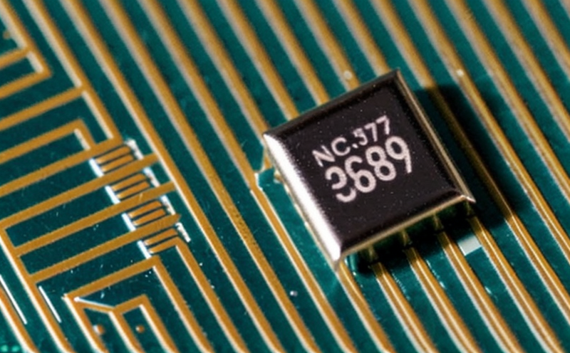
ASTM F1400 Low-k Dielectric Integrity Testing
The ASTM F1400 standard is a critical tool in semiconductor and microchip testing, specifically focusing on the integrity of low-k dielectrics. Low-k materials are crucial in modern integrated circuits (ICs) as they provide lower capacitance per unit area compared to traditional silicon dioxide, enabling smaller and faster chips. The ASTM F1400 test evaluates the mechanical stability and reliability of these materials under various conditions that mimic real-world applications.
The primary objective of this testing is to ensure that low-k dielectric layers within microchips can withstand the stresses encountered during manufacturing processes such as etching, deposition, and packaging. By adhering to ASTM F1400 standards, manufacturers can guarantee the long-term reliability and performance of their ICs.
The testing procedure involves subjecting the specimen to mechanical stress through a series of controlled physical tests. These include peel tests, shear strength evaluations, and bend tests designed to simulate the stresses that low-k layers undergo during assembly. The ASTM F1400 standard provides specific criteria for these tests, ensuring consistent and accurate results.
One of the key aspects of this testing is the use of a cross-sectional scanning electron microscopy (SEM) analysis. SEM allows for detailed examination of the specimen's structure at various depths, enabling the identification of any defects or changes in material integrity. This non-destructive technique provides invaluable insights into the quality and consistency of the low-k layer.
Another critical factor is the environmental conditions under which the tests are conducted. These include temperature cycling to simulate operational environments and humidity exposure to assess the impact on dielectric properties. By incorporating these elements, ASTM F1400 ensures a comprehensive evaluation that reflects real-world use scenarios.
The results of ASTM F1400 testing are vital for quality managers and compliance officers in semiconductor manufacturing. These tests provide critical data that can influence design choices, process improvements, and material selection. R&D engineers rely on these test outcomes to optimize the performance and durability of microchips. For procurement teams, the standard offers a reliable benchmark for evaluating supplier capabilities.
By adhering to ASTM F1400 standards, manufacturers not only meet regulatory requirements but also enhance their reputation in the market by delivering high-quality products that are trusted for long-term reliability. The standard's rigorous methodology ensures consistent and reproducible results, which is essential for the semiconductor industry's advancement.
Scope and Methodology
| Test Type | Description |
|---|---|
| Pull Test | Evaluates the bond strength between the low-k dielectric layer and adjacent materials. |
| Bend Test | Assesses the flexibility of the low-k layer under mechanical stress without compromising its integrity. |
| Shear Strength Evaluation | Determines the resistance to shear forces, which can occur during assembly processes. |
| SEM Analysis | Provides a detailed cross-sectional view of the low-k layer to identify any defects or inconsistencies. |
The ASTM F1400 standard outlines a series of mechanical and environmental tests designed to evaluate the integrity of low-k dielectric layers. These include pull tests, bend tests, shear strength evaluations, and SEM analysis. Each test is conducted under controlled conditions that simulate real-world stressors, ensuring accurate and reliable results.
The testing process begins with the preparation of the specimen, which involves creating a cross-section of the low-k layer for SEM analysis. This step is crucial as it allows for detailed examination of any defects or inconsistencies within the material. Following this, the specimen undergoes mechanical tests to assess its bond strength and flexibility under stress.
Environmental conditions play a significant role in the testing process. The specimen is subjected to temperature cycling to simulate operational environments and humidity exposure to evaluate the impact on dielectric properties. These environmental stresses are critical as they can significantly affect the performance of low-k layers over time.
Benefits
The implementation of ASTM F1400 Low-k Dielectric Integrity Testing brings several benefits to semiconductor manufacturers and R&D engineers. Firstly, it ensures consistent quality across production batches, providing confidence in product reliability. Secondly, the testing process identifies potential issues early in the manufacturing cycle, allowing for timely corrections and improvements.
For quality managers and compliance officers, ASTM F1400 offers a robust framework to ensure regulatory compliance while enhancing product performance. This standard is widely recognized by industry stakeholders, making it easier to integrate into existing quality management systems.
R&D engineers can leverage the results of this testing to optimize design parameters and material selection. By identifying areas of improvement through ASTM F1400 testing, they can develop more robust and reliable microchips. Additionally, the standard's rigorous methodology ensures reproducible results, enabling consistent performance across different production runs.
From a procurement perspective, adherence to ASTM F1400 provides assurance that suppliers meet stringent quality standards. This reduces the risk of receiving substandard materials and ensures that all components used in manufacturing align with industry best practices.
In summary, ASTM F1400 Low-k Dielectric Integrity Testing is essential for maintaining high-quality standards in semiconductor manufacturing. It supports continuous improvement by identifying potential issues early on and ensuring consistent performance across production batches. The standard's recognition within the industry also enhances trust between manufacturers and their supply chain partners.
International Acceptance and Recognition
- ASTM F1400 is recognized globally for its stringent testing criteria, aligning with international standards such as ISO 9001.
- The standard is widely adopted by semiconductor manufacturers to ensure product reliability and quality.
- ASTM F1400 compliance is a key requirement in many global markets, including North America, Europe, and Asia-Pacific regions.
- Industry stakeholders frequently use ASTM F1400 as the benchmark for evaluating supplier capabilities and product performance.
The ASTM F1400 standard's recognition extends beyond individual manufacturers to encompass entire supply chains. Its global acceptance ensures that products meeting this standard are trusted across diverse markets, enhancing their competitiveness in international trade.
By adhering to ASTM F1400 standards, semiconductor manufacturers can demonstrate their commitment to quality and reliability, thereby fostering trust among customers and partners. The standard's widespread adoption also facilitates smoother regulatory compliance processes, reducing the time and effort required for market entry.


