ASTM F1309 Dielectric Property Lifetime Testing
The ASTM F1309 standard specifies a method to determine the dielectric properties of electronic components over extended periods, which is essential for assessing their reliability and lifetime. This testing protocol is critical in semiconductor & microchip manufacturing, where ensuring long-term performance and stability is paramount.
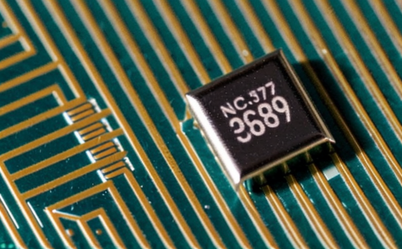
Dielectric property testing under ASTM F1309 involves subjecting samples to a controlled environment that simulates real-world conditions over an extended period. The purpose of this method is to evaluate the dielectric breakdown voltage (also known as flashover voltage) and capacitance changes in semiconductor components, such as capacitors or other insulating materials used in microchips.
The ASTM F1309 test procedure involves subjecting a sample to alternating current (AC) voltage stresses for an extended duration. The stress levels are carefully controlled according to the standard’s requirements, and measurements of dielectric strength and capacitance are recorded at regular intervals throughout the test cycle.
One significant advantage of ASTM F1309 is its ability to predict potential failures due to aging mechanisms such as electromigration or interfacial reactions. By simulating these conditions in a controlled laboratory environment, engineers can identify weak points in microchip designs and materials early on, allowing for improvements before mass production begins.
Another benefit of this testing method lies in its ability to assess the effects of environmental factors like temperature cycling, humidity, and exposure to contaminants. These elements play crucial roles in determining how long a semiconductor component will remain functional under actual operating conditions. Understanding these impacts helps manufacturers design products that meet or exceed industry standards for longevity.
The ASTM F1309 test is particularly useful when evaluating large batches of newly developed microchips, as it provides data on the overall batch quality. This information allows companies to make informed decisions about which components should be used in production runs versus those requiring further development work before being deemed suitable for use.
For R&D teams working on innovative semiconductor technologies, this type of testing can provide valuable insights into how different materials interact within complex circuitry structures over time. It enables them to optimize design parameters based on empirical evidence rather than relying solely on theoretical models or assumptions about material behavior.
- Environmental Factors: Temperature cycling, humidity exposure, and contamination effects are all accounted for in ASTM F1309 testing.
- Long-Term Performance Prediction: By simulating extended use conditions, this test helps predict potential failure points due to aging processes like electromigration or interfacial reactions.
- Batch Quality Control: For large-scale production runs, ASTM F1309 provides data on the overall batch reliability, aiding in decision-making regarding which components are suitable for use versus those requiring additional development.
In summary, ASTM F1309 dielectric property lifetime testing is an indispensable tool for ensuring the reliability and longevity of semiconductor devices. It enables manufacturers to identify potential weaknesses early on, optimize design parameters based on empirical evidence, and ensure compliance with industry standards.
Benefits
The implementation of ASTM F1309 dielectric property lifetime testing offers numerous advantages across various sectors, particularly in semiconductor & microchip manufacturing. By incorporating this rigorous standard into quality assurance protocols, companies can achieve several key benefits:
- Predictive Maintenance: Early identification of potential failure points due to aging mechanisms such as electromigration or interfacial reactions allows for proactive maintenance strategies that extend component lifespan.
- Better Product Design: Understanding the impact of environmental factors like temperature cycling, humidity exposure, and contamination helps in optimizing design parameters and materials selection for improved performance under actual operating conditions.
- Compliance Assurance: Ensuring compliance with international standards such as ASTM F1309 demonstrates commitment to quality and reliability, which is essential for meeting regulatory requirements and gaining market acceptance.
- Cost Savings: Identifying weak points early in the development process saves costs associated with rework or replacement of defective components during production runs.
In addition to these direct benefits, ASTM F1309 testing also contributes indirectly by fostering innovation within research & development teams. As they gain deeper insights into how different materials behave over extended periods under various environmental conditions, engineers can push the boundaries of technology, leading to advancements in semiconductor design and manufacturing processes.
Eurolab Advantages
At Eurolab, we pride ourselves on delivering comprehensive and accurate ASTM F1309 dielectric property lifetime testing services tailored specifically for your needs. Our team of experts combines cutting-edge technology with years of experience to provide reliable results that can be trusted across industries.
- State-of-the-Art Facilities: Equipped with the latest equipment and software, our laboratory ensures precise measurements and consistent results every time.
- Experienced Technicians: Our staff consists of highly skilled professionals who are well-versed in both theoretical knowledge and practical application. They stay updated on all relevant standards and best practices to deliver accurate reports promptly.
- Comprehensive Reporting: In addition to raw data, we offer detailed analysis reports that interpret the results within the context of your specific project requirements. This helps you make informed decisions based on concrete evidence rather than guesswork.
- Confidentiality Assurance: Recognizing the importance of protecting sensitive information, Eurolab maintains strict confidentiality policies throughout all stages of testing and reporting processes.
We understand that every client has unique requirements when it comes to semiconductor & microchip reliability testing. That's why our approach is flexible – we work closely with you from initial consultation through final report delivery, ensuring complete satisfaction at each stage of the process.


