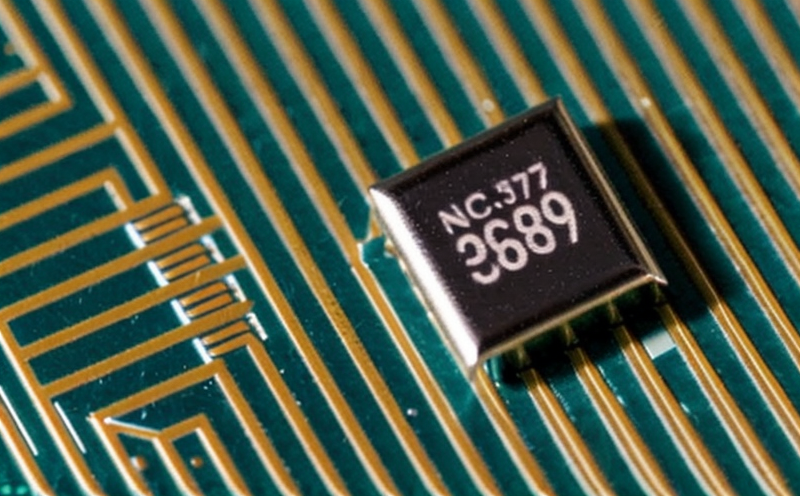
JEDEC JESD22-A135 Microchip Dielectric Integrity Testing
The JEDEC Standard JESD22-A135 is a critical procedure used to evaluate the dielectric integrity of microchips, ensuring they can withstand high-voltage stress without degradation or failure. This test is essential for semiconductor manufacturers and quality assurance teams as it helps identify potential defects that could lead to long-term reliability issues.
The standard outlines a method for applying a direct current voltage across a specimen, typically in the form of a microchip die mounted on a printed circuit board (PCB), and then monitoring the leakage current. The test aims to stress the insulating layer between the conductive layers within the chip, simulating real-world conditions that might be encountered during use.
One key aspect of this testing method is its ability to detect insulation breakdown or other forms of failure in the dielectric materials used in microchips. These materials are crucial for maintaining signal integrity and preventing short circuits between conductive layers. By subjecting these layers to high voltage, the test can identify weaknesses that may not be apparent during initial manufacturing checks.
The procedure involves placing the specimen into a fixture designed specifically for JESD22-A135 testing. The fixture ensures consistent contact with both the power supply and measurement equipment while also providing support necessary for accurate voltage application and current measurement. Once positioned, the device is connected to a high-voltage source capable of delivering controlled levels of stress.
The test begins by applying a specified voltage gradually, starting at a low level and increasing incrementally until it reaches either a predetermined threshold or a point where insulation breakdown occurs. Throughout this process, careful monitoring of leakage current allows technicians to observe any changes indicative of potential problems within the dielectric structure. If no failure is detected up to 2,000 volts, additional tests may be conducted using lower voltages.
Post-testing analysis focuses on interpreting both visual and numerical data collected during the experiment. Visual inspection checks for signs such as charring or physical damage at the test site, while numerical evaluation examines parameters like peak current values and time-to-breakdown metrics to determine compliance with relevant specifications outlined in JESD22-A135.
Compliance with this standard ensures that manufacturers produce reliable semiconductor products capable of performing consistently over extended periods under various environmental conditions. For quality managers, compliance officers, R&D engineers, and procurement professionals involved in selecting components for their projects, understanding the importance of dielectric integrity testing cannot be overstated. Proper implementation helps prevent costly failures later on by catching issues early in development cycles.
Using JESD22-A135 ensures adherence to industry best practices recommended by leading organizations like JEDEC, ensuring consistent performance across all units produced. This standard plays a vital role in maintaining high standards of reliability and quality within the semiconductor manufacturing sector.
Applied Standards
The JEDEC JESD22-A135 Microchip Dielectric Integrity Testing aligns closely with international standards designed to ensure robust performance across diverse applications. Key references include:
- JESD22-A135: This standard specifies the methodology for testing the dielectric integrity of semiconductor devices using a direct current voltage stress technique.
- ISO 7649:2008: Provides guidelines on insulation resistance tests which complement JESD22-A135 by offering broader insights into material properties relevant to electrical insulation systems.
- ASTM D257-17: Focuses on measuring dielectric strength and dissipation factor of solid insulating materials, providing additional context for interpreting results from JESD22-A135.
By incorporating these standards into the testing protocol, laboratories ensure comprehensive evaluation that meets global regulatory requirements. This approach enhances confidence in test outcomes among stakeholders involved in semiconductor design and production processes.
Scope and Methodology
The scope of JESD22-A135 encompasses various types of microchips used in electronic devices, including but not limited to:
- Digital Signal Processors (DSPs)
- Application Specific Integrated Circuits (ASICs)
- Microcontrollers
- Power Management ICs (PMICs)
This testing procedure is particularly important for ensuring that the insulating layers between conductive traces and pads are sufficiently robust to withstand operational stresses without compromising functionality. The methodology involves several key steps:
- Specimen Preparation: Chips are carefully prepared by mounting them on a PCB according to prescribed procedures outlined in JESD22-A135.
- Fixture Assembly: Specimens are inserted into fixtures that maintain precise alignment and secure contact with the voltage source and measurement equipment.
- Voltage Application: A controlled voltage is applied across the specimen, starting at a low level before gradually increasing to stress the insulating materials.
- Current Measurement: Simultaneous monitoring of leakage current provides real-time data on how well the insulation holds up under applied stress.
- Data Analysis: Post-test analysis involves reviewing both visual and numerical results to assess compliance with specified limits.
The entire process is designed to provide comprehensive assessment of dielectric integrity, enabling manufacturers to make informed decisions about product improvements based on scientific evidence derived from rigorous testing procedures.
Competitive Advantage and Market Impact
Adherence to the JEDEC JESD22-A135 standard offers numerous competitive advantages for semiconductor companies operating in a highly competitive market. Firstly, it enhances brand reputation by demonstrating commitment to quality and reliability standards recognized globally.
By ensuring consistent performance across all units produced, firms can reduce warranty claims and improve customer satisfaction levels. This ultimately translates into increased market share as satisfied customers become repeat buyers or recommend products to others.
The ability to meet stringent testing protocols also opens doors to new business opportunities within niche markets that prioritize reliability above cost considerations. For instance, aerospace and defense sectors often require extremely robust components capable of functioning reliably under extreme conditions. Compliance with JESD22-A135 helps secure contracts from such demanding clients.
Moreover, adopting this standard fosters innovation by encouraging continuous improvement in materials science and manufacturing processes aimed at enhancing dielectric integrity further. Such advancements not only bolster current products but also lay foundations for future generations of more advanced chips.
In conclusion, embracing the JEDEC JESD22-A135 Microchip Dielectric Integrity Testing is not just a compliance requirement; it represents an investment in long-term success through superior product quality and competitive edge.


