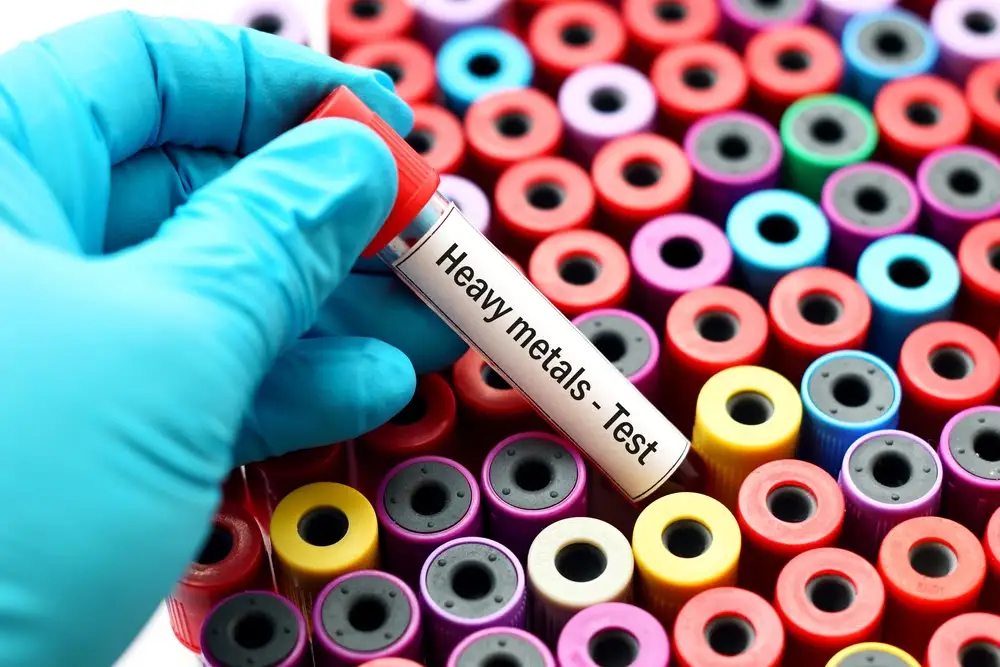
Semiconductor Heavy Metal Testing
At Eurolab, our Semiconductor Heavy Metal Testing service ensures that your semiconductor products meet stringent safety and quality standards. This critical testing is essential to identify the presence of heavy metals such as lead (Pb), mercury (Hg), cadmium (Cd), chromium (Cr), and arsenic (As) in semiconductors. These elements are hazardous if present in excessive amounts, posing risks to both human health and the environment.
The semiconductor industry is highly regulated due to the potential toxicity of heavy metals used during manufacturing processes. Compliance with international standards such as ISO 17025, ASTM E586-13, and IEC 62391 is crucial for manufacturers to ensure product safety and reliability.
The testing process involves several key steps, including the preparation of semiconductor samples. This requires meticulous handling to avoid cross-contamination and ensure accurate results. Our laboratory adheres strictly to industry best practices, ensuring that each sample is prepared in a controlled environment. Once prepared, the samples undergo analysis using state-of-the-art instrumentation such as Inductively Coupled Plasma Mass Spectrometry (ICP-MS) and Energy Dispersive X-ray Spectroscopy (EDX).
The results of these tests are meticulously documented, providing detailed information on the levels of heavy metals present in each semiconductor product. These reports serve as a critical tool for quality assurance teams to make informed decisions regarding production processes and material sourcing.
Our commitment to accuracy is further enhanced by our experienced team of scientists and engineers who have deep expertise in materials science and analytical chemistry. They work closely with clients to understand their specific needs and provide tailored testing solutions. This collaborative approach ensures that the testing process aligns perfectly with your unique requirements, whether you are a manufacturer looking to ensure compliance or an R&D engineer seeking insights into material composition.
The importance of this service cannot be overstated in today’s regulatory landscape. Non-compliance can lead to significant financial penalties and reputational damage. By partnering with Eurolab for your semiconductor heavy metal testing, you can rest assured that your products meet the highest safety standards and are free from harmful contaminants.
Scope and Methodology
Semiconductor Heavy Metal Testing encompasses a comprehensive approach to identifying and quantifying heavy metals in semiconductor materials. The testing scope includes the following key areas:
| Sample Types | Ingot, wafer, die, and finished product. |
| Heavy Metals Tested | Pb, Hg, Cd, Cr, As. |
| Testing Techniques | ICP-MS, EDX. |
| Compliance Standards | ISO 17025, ASTM E586-13, IEC 62391. |
| Acceptance Criteria | Levels of heavy metals must not exceed regulatory limits set by international standards. |
The methodology for this testing involves several critical steps:
Sample Preparation: Ensuring that the sample is representative and free from contamination. This step includes cleaning, cutting, and grinding of samples to obtain a homogenous specimen.
Analytical Procedures: Utilizing advanced instrumentation such as ICP-MS and EDX for precise measurement. These instruments provide high sensitivity and accuracy, allowing us to detect even trace amounts of heavy metals.
Data Analysis: Interpretation of data obtained from the analysis is crucial. Our team employs statistical methods to ensure that results are reliable and reproducible.
Reporting: Comprehensive reports are generated detailing all findings, including levels of detected heavy metals and compliance with relevant standards.
EuroLab Advantages
Partnering with Eurolab for your Semiconductor Heavy Metal Testing offers numerous advantages:
- Expertise and Experience: Our team comprises highly skilled professionals with extensive experience in materials science and analytical chemistry.
- State-of-the-Art Facilities: Access to cutting-edge laboratories equipped with the latest instrumentation ensures accurate and reliable results.
- Comprehensive Services: From sample preparation to final report generation, we provide a seamless testing process tailored to your needs.
- Dedicated Client Support: Our team is always available to address any questions or concerns you may have throughout the testing process.
- Regulatory Compliance: Ensuring that all tests meet the stringent requirements set by international standards such as ISO 17025, ASTM E586-13, and IEC 62391.
- Confidentiality: We maintain strict confidentiality of your data to protect sensitive information.
These advantages make Eurolab the premier choice for semiconductor heavy metal testing. Our commitment to quality and accuracy sets us apart in the industry, ensuring that you receive reliable results every time.
Why Choose This Test
The importance of Semiconductor Heavy Metal Testing cannot be overstated. Here’s why:
Regulatory Compliance: Ensuring compliance with international standards is essential to avoid legal penalties and maintain a positive reputation.
Risk Management: Identifying and mitigating risks associated with heavy metal contamination helps protect your brand and consumer trust.
Quality Assurance: Accurate testing ensures that only high-quality products reach the market, enhancing overall product reliability.
Innovation: Understanding the composition of materials can drive innovation in semiconductor design and manufacturing processes.
Safety: Preventing exposure to harmful heavy metals is crucial for both human health and environmental protection.
By choosing Eurolab, you are investing in the future success of your semiconductor products. Our rigorous testing ensures that your materials meet the highest safety standards, allowing you to focus on other critical aspects of product development.


