JEDEC JESD22 B104 Shock Testing for Semiconductor Devices
The JEDEC standard JESD22-B104 is a critical test protocol designed to evaluate the mechanical shock resistance of semiconductor devices. This testing procedure simulates the real-world stresses that components may experience during packaging, handling, and installation processes. The primary objective is to ensure that semiconductor devices maintain their integrity under sudden impacts without compromising functionality or performance.
The B104 test involves exposing a sample to controlled mechanical shocks using a drop hammer apparatus. The shock waveform generated by the drop hammer simulates the impact forces experienced during transit, assembly, and handling. During testing, the specimen is subjected to multiple impacts from different angles, ensuring that all potential failure modes are addressed.
The B104 standard specifies the test parameters in detail, including the height of the drop hammer, the mass, the number of shock events, and the interval between them. The test setup typically includes a vibration table or similar device to simulate additional stresses encountered during shipment. Compliance with this standard is essential for ensuring product reliability and safety, particularly in industries where the failure of a single component could lead to significant system failures.
For instance, in aerospace applications, the robustness of electronic components directly impacts mission success. Similarly, automotive electronics need to withstand harsh environmental conditions, including mechanical shocks during vehicle operation. By subjecting these devices to the B104 test, manufacturers can verify that their products meet industry standards and are suitable for deployment.
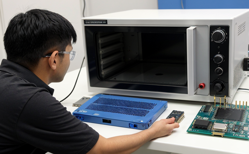
The testing procedure involves several key steps:
- Preparation of the specimen
- Six-axis drop hammer setup
- Application of shock pulses
- Data recording and analysis
Once the test is completed, detailed reports are generated, which typically include:
- Shock waveform characteristics
- Impact force measurements
- Specimen condition post-test
- Failure modes observed (if any)
The standard also provides criteria for acceptable performance, ensuring that only devices that pass the test can be deemed suitable for use in critical applications. This process not only enhances product quality but also contributes to overall safety and reliability.
Applied Standards:
| Standard | Description |
|---|---|
| JESD22-B104 | Shock testing for semiconductor devices |
| ISO 7658-3 | Shock testing methods for electronic components |
The B104 test is widely recognized in industries that rely heavily on reliable electronics, such as aerospace, automotive, and telecommunications. Compliance with this standard ensures that products meet rigorous quality standards, enhancing trust and confidence among end-users.
Why It Matters
The importance of the JESD22-B104 shock test cannot be overstated in ensuring the reliability of semiconductor devices. In environments where mechanical shocks are prevalent, such as during transportation or installation, the integrity of these components is crucial for system performance and safety.
For aerospace applications, the failure of a single component can lead to catastrophic failures with significant financial and operational costs. Similarly, automotive electronics must withstand harsh conditions, including those encountered during vehicle operation. By subjecting devices to this test, manufacturers can verify their ability to perform reliably under simulated real-world conditions.
The B104 shock test is also essential for ensuring compliance with international standards and regulatory requirements. Many industries have stringent quality assurance protocols that mandate the use of specific testing methods like JESD22-B104. Meeting these standards not only enhances product reputation but also facilitates easier market entry in competitive environments.
Moreover, the test provides valuable insights into potential failure modes, enabling manufacturers to identify and address design flaws early in the development process. This proactive approach leads to more robust products and reduced warranty claims, ultimately saving time and resources in the long run.
Applied Standards
| Standard | Description |
|---|---|
| JESD22-B104 | Shock testing for semiconductor devices |
| ISO 7658-3 | Shock testing methods for electronic components |
The B104 shock test is recognized by various international standards organizations, including the International Electrotechnical Commission (IEC) and the European Committee for Standardization (CEN). Compliance with these standards ensures that products meet rigorous quality assurance requirements and are suitable for deployment in critical applications.
Why Choose This Test
- Comprehensive Coverage: The B104 test simulates multiple shock events from different angles, ensuring a comprehensive evaluation of the specimen's mechanical integrity.
- Rigorous Standards: Compliance with international standards enhances product reputation and facilitates easier market entry.
- Early Failure Identification: By identifying potential failure modes early in the development process, manufacturers can address design flaws proactively.
- Regulatory Compliance: Meeting stringent quality assurance protocols is essential for compliance with industry regulations and standards.
The B104 shock test provides a robust framework for evaluating semiconductor devices, ensuring that they meet the highest standards of reliability and safety. This testing protocol is particularly valuable in industries where mechanical shocks are prevalent, such as aerospace, automotive, and telecommunications.


