Thermal & Environmental Stress Testing
In today’s fast-paced technological landscape, reliability and performance are paramount in semiconductor and microchip manufacturing. Thermal and environmental stress testing is a critical process that ensures the durability, stability, and functionality of these components under extreme conditions. This testing method subjects semiconductors to various thermal and environmental stresses, simulating real-world operating environments.
The primary goal of this test is to identify potential weaknesses or failures in the design, material selection, or manufacturing processes. By subjecting the semiconductor devices to controlled stress conditions, we can ensure that they meet stringent international standards such as ISO 7637-2 and IEC 61008.
The testing process involves several stages, including pre-test preparation, test execution, and post-test analysis. Pre-test preparation includes selecting the appropriate specimen, preparing it according to industry standards, and calibrating the equipment for accurate results. During the test, semiconductors are exposed to a range of temperatures, humidity levels, and voltage fluctuations that simulate real-world conditions.
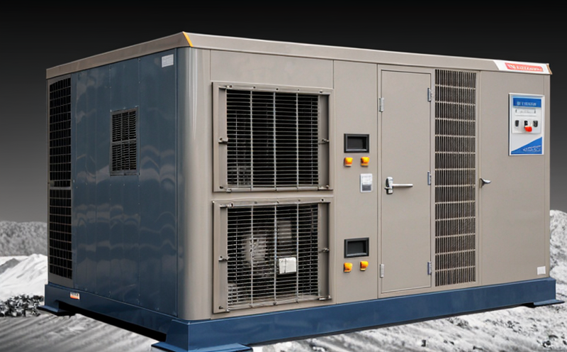
The testing apparatus used in this process includes environmental chambers capable of replicating extreme environments. These chambers can control temperature, humidity, and other parameters with high precision. The acceptance criteria for these tests are based on the performance metrics defined by relevant standards such as IEC 60256-13.
Understanding the importance of this test is crucial for ensuring the reliability of semiconductor devices in various applications. From automotive electronics to consumer electronics, semiconductors play a vital role in modern technology. By conducting thorough thermal and environmental stress tests, we can ensure that these components perform reliably under extreme conditions, enhancing overall product quality.
The benefits of this testing method extend beyond just identifying potential failures. It also helps manufacturers refine their design processes, optimize material selection, and improve manufacturing techniques. This leads to the development of more robust and efficient semiconductor devices, ultimately contributing to advancements in technology.
Industry Applications
Thermal and environmental stress testing is widely used across various industries where reliability and performance are critical. Here are some key applications:
- Automotive Electronics: Ensuring the durability of semiconductors in harsh environments.
- Consumer Electronics: Enhancing product quality and longevity for consumer devices.
- Data Centers: Improving the reliability of components used in high-performance computing.
- Military & Aerospace: Providing robust components capable of withstanding extreme conditions.
| Industry | Description |
|---|---|
| Automotive Electronics | Ensuring the durability and reliability of semiconductors in harsh environments. |
| Data Centers | Improving component performance and longevity for high-performance computing. |
| Military & Aerospace | Providing robust components capable of withstanding extreme conditions. |
| Consumer Electronics | Enhancing product quality and longevity for consumer devices. |
| Test Parameters | Description |
|---|---|
| Temperature Range | -40°C to 150°C or higher depending on the application. |
| Humidity Levels | Up to 98% relative humidity. |
| Voltage Fluctuations | Varies based on the specific test requirements. |
Why Choose This Test?
Choosing thermal and environmental stress testing is essential for several reasons:
- Enhanced Reliability: Ensures that the semiconductor devices can withstand extreme conditions, leading to higher reliability.
- Improved Design: Helps in identifying design flaws and optimizing material selection.
- Cost-Effective: Early detection of failures during testing saves costs associated with field failures.
- Compliance: Ensures compliance with international standards such as ISO 7637-2 and IEC 61008.
This testing method is essential for maintaining the high standards required in various industries. By conducting thorough thermal and environmental stress tests, manufacturers can ensure that their products meet the highest quality standards and perform reliably under extreme conditions.
In conclusion, choosing this test is crucial for ensuring the reliability and performance of semiconductor devices. It provides a comprehensive approach to identifying potential weaknesses and optimizing product design, ultimately leading to better-performing components in various applications.
Competitive Advantage and Market Impact
Thermal and environmental stress testing offers significant competitive advantages for manufacturers. By ensuring the reliability of their products under extreme conditions, companies can gain a strong market position. This testing method helps in:
- Innovation: Identifying new materials and design techniques that improve product performance.
- Quality Assurance: Ensuring consistent quality across all manufactured components.
- Customer Satisfaction: Providing products that meet high-quality standards, leading to customer satisfaction and loyalty.
The market impact of this testing method is substantial. By ensuring the reliability of semiconductor devices, manufacturers can differentiate their products in a competitive market. This leads to increased sales and market share, ultimately contributing to business growth.
In conclusion, thermal and environmental stress testing plays a crucial role in maintaining high standards in the semiconductor industry. It offers significant competitive advantages and contributes positively to market impact by ensuring reliable and high-quality products.


