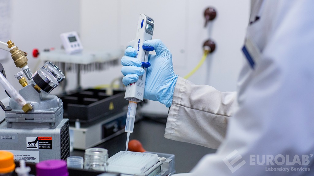
Semiconductor Material Inorganic Residue Check
The semiconductor industry demands stringent quality control to ensure the reliability and performance of electronic components. One critical aspect of this control is the inorganic residue check on semiconductor materials. This process ensures that any unwanted inorganic compounds are identified, quantified, and removed before they can affect the material's integrity or functionality.
The presence of even trace amounts of inorganic residues can lead to contamination issues that compromise device performance. For instance, metals like iron, copper, or aluminum can interact with other semiconductor materials, leading to short circuits or reduced conductivity. Therefore, it is essential to perform a thorough check to verify the cleanliness and purity of the material.
The test typically involves several steps: initial sample preparation, dissolution using appropriate solvents, filtration, and final analysis by techniques such as Inductively Coupled Plasma Mass Spectrometry (ICP-MS), Atomic Absorption Spectroscopy (AAS), or Infrared Spectroscopy (IR). These methods allow for precise quantification of inorganic elements down to parts per billion levels.
The testing process is not only about identifying residues but also ensuring that the material meets specific purity standards set by international bodies like ISO and ASTM. Compliance with these standards ensures that the materials are suitable for use in high-reliability applications such as microprocessors, memory chips, and power semiconductors.
Real-world applications of this test include:
- Supply Chain Management: Ensuring that all incoming semiconductor materials meet purity specifications to prevent contamination issues downstream.
- R&D Optimization: Identifying sources of impurities that could impact the development process, leading to more robust and reliable products.
- Manufacturing Process Monitoring: Continuous testing during production ensures consistent quality and eliminates batch-to-batch variability.
- Compliance Verification: Demonstrating adherence to industry standards and regulations for regulatory approval processes.
The process also involves strict sample preparation techniques, which are crucial in obtaining accurate results. Samples must be carefully cleaned and prepared according to standardized procedures to avoid introducing additional contaminants. This meticulous approach ensures that the test results reflect only the true nature of the material being analyzed.
Another key aspect is the use of advanced analytical instruments capable of detecting even minute levels of impurities. The precision of these instruments allows for accurate quantification, which is vital for meeting stringent industry requirements. For example, some modern ICP-MS systems can detect elements at parts per trillion (ppt) concentrations.
Understanding international standards is essential when performing this test. ISO 8460 and ASTM E1259 provide guidelines for the sampling, handling, and analysis of semiconductor materials. Adhering to these standards ensures that the testing process is consistent across different laboratories and regions.
In summary, the inorganic residue check on semiconductor materials is a critical step in ensuring product quality and reliability. By meticulously following standardized procedures and using advanced analytical techniques, this test helps prevent contamination issues that could otherwise lead to significant performance degradation or failure of electronic devices.
Applied Standards
The application of international standards is crucial for accurate and consistent testing in the semiconductor industry. The most relevant standards include:
- ASTM E1259-08(2016): Standard Practice for Sampling, Handling, and Analysis of Silicon Wafer Material: This standard provides comprehensive guidelines on how to sample, handle, and analyze silicon wafer materials. It ensures that the testing process is standardized across different laboratories.
- ISO 8460: Semiconductor devices - General requirements for semiconductor material: This international standard specifies general requirements for semiconductor materials used in electronic components. Compliance with this standard guarantees that the materials meet industry-wide quality expectations.
- ASTM E1725-18(2023): Standard Practice for Sampling, Handling and Analysis of Gallium Arsenide (GaAs) Materials: This specific standard addresses the unique properties and handling requirements of GaAs materials. It ensures that these materials are tested accurately and consistently.
- ISO 9478: Semiconductor devices - General requirements for semiconductor material: Another international standard that specifies general requirements for semiconductor materials, ensuring consistent quality across different manufacturers and suppliers.
The use of these standards ensures that the testing process is standardized, leading to reliable and reproducible results. Compliance with these standards also enhances credibility and trustworthiness within the industry, as they are recognized globally by regulatory bodies and other stakeholders.
Why Choose This Test
The importance of an inorganic residue check on semiconductor materials cannot be overstated, particularly for high-performance applications. Here are some reasons why this test is essential:
- Avoidance of Contamination: Even trace amounts of inorganic residues can lead to contamination issues that affect device performance.
- Enhanced Product Quality: Ensuring that the material meets strict purity standards results in higher-quality products with improved reliability and longevity.
- Compliance with Industry Standards: Adhering to international standards like ISO 8460 and ASTM E1259 ensures compliance with industry regulations and expectations.
- Cost Efficiency: Early detection of impurities can prevent costly rework or scrap, saving time and resources in the long run.
- Enhanced Reputation: Consistent quality control demonstrates a commitment to excellence and builds trust among customers and partners.
- Innovation Support: Identifying sources of contamination allows for continuous improvement in manufacturing processes, driving innovation within the industry.
The test is particularly valuable for companies operating at the cutting edge of technology. By maintaining a high level of purity in their materials, they can ensure that their products meet or exceed market demands and regulatory requirements. This commitment to quality not only enhances product performance but also fosters customer satisfaction and loyalty.
International Acceptance and Recognition
The semiconductor industry is global, with suppliers and manufacturers operating across different regions. As a result, the inorganic residue check on semiconductor materials must be internationally recognized to ensure consistency and reliability. Here’s why international acceptance and recognition are crucial:
- Global Standards: International standards like ISO 8460 and ASTM E1259 provide uniform guidelines for testing, ensuring that the results are accepted worldwide.
- Regulatory Compliance: Many countries have regulations requiring compliance with international standards. Ensuring that your tests meet these standards is essential for regulatory approval.
- Market Access: International recognition opens up opportunities to participate in global markets, enhancing business prospects and growth potential.
- Collaboration Opportunities: Recognized testing methods facilitate collaboration between suppliers, manufacturers, and research institutions across borders.
- Reputation Building: Consistent quality control that adheres to international standards enhances the reputation of your company within the industry.
The global nature of the semiconductor industry means that any discrepancies in testing methods or results can lead to significant challenges. By ensuring that all testing is conducted according to internationally recognized standards, companies can avoid these issues and maintain a competitive edge in the market.


