Semiconductor device inspection
At Eurolab, we specialize in providing comprehensive semiconductor device inspections to ensure that electronic components meet stringent quality and performance standards. This service is critical for industries relying on reliable microelectronics, such as automotive, aerospace, telecommunications, and consumer electronics.
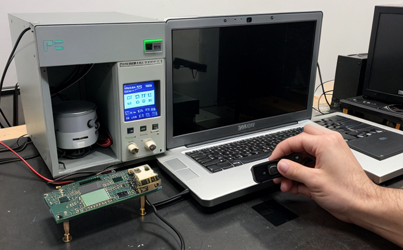
The process begins with a thorough inspection of the semiconductor devices using high-resolution scanning electron microscopy (SEM) and optical microscopy. Our experienced technicians examine each component to identify defects that could impact performance or reliability. This includes checking for surface contaminants, cracks, and other physical imperfections that might affect device functionality.
For more complex inspections, we utilize advanced testing methods such as cross-section analysis using focused ion beam (FIB) technology. This allows us to examine the internal structure of devices at an atomic level, ensuring that all layers are correctly formed and that there are no hidden defects. Additionally, our laboratory adheres to international standards like ISO 17025 for quality assurance, ensuring that every test is conducted under controlled conditions.
The use of advanced instrumentation ensures not only precision but also reproducibility in our results. Our state-of-the-art facilities incorporate equipment from leading manufacturers such as FEI and Hitachi. These tools allow us to perform tests according to various standards including IEC 60312 for power semiconductor devices and JIS C 8352 for diodes, among others.
Our approach extends beyond mere inspection; it includes predictive analytics based on historical data collected during inspections. By analyzing trends over time, we can anticipate potential issues before they become critical failures, helping our clients maintain optimal performance and reduce downtime.
The importance of semiconductor device inspection cannot be overstated in today’s tech-driven world where even minor deviations can lead to catastrophic consequences. From ensuring compliance with industry regulations to enhancing product longevity and safety, Eurolab offers a robust solution tailored specifically for this demanding field.
- Ensures adherence to international standards
- Reduces the risk of component failure in critical applications
- Promotes longer lifespan of electronic devices through early defect detection
- Supports regulatory compliance across multiple sectors
- Improves overall quality control within manufacturing processes
- Aids in troubleshooting complex electrical issues effectively and efficiently
By leveraging our expertise, clients can rest assured that their semiconductor components are free from defects and ready for deployment. This commitment to excellence sets Eurolab apart as a trusted partner in the realm of semiconductor device inspection.
Benefits
- Achieve higher product quality and reliability
- Promote safer operation of electronic devices
- Enhance brand reputation through consistent performance standards
- Minimize costs associated with rework or replacement due to faulty components
- Facilitate faster time-to-market by ensuring products meet all necessary criteria early in development stages
- Safeguard against potential legal liabilities resulting from non-compliant products
The benefits of semiconductor device inspection extend far beyond mere quality assurance. By incorporating this service into your workflow, you ensure that only the highest-quality components are used within your manufacturing processes.
Why Choose This Test
- State-of-the-art equipment ensures accurate and reliable inspections
- Comprehensive coverage of international standards guarantees compliance
- Dedicated team of experts provides detailed insights into each inspection result
- Robust support services including training and consultation enhance understanding and implementation
- Prompt turnaround times facilitate quicker decision-making and smoother production processes
- Strong reputation in the industry built on years of successful inspections and satisfied clients
Selecting Eurolab for your semiconductor device inspection needs means partnering with a leader in precision engineering. Our commitment to excellence ensures that you receive the best possible outcome from every test performed.
Eurolab Advantages
At Eurolab, we pride ourselves on offering unparalleled service and exceptional results when it comes to semiconductor device inspection. With years of experience and cutting-edge technology at our disposal, we provide a level of expertise that few others can match.
- Experienced and knowledgeable staff
- Pioneering use of advanced instrumentation
- Certification and accreditation from leading authorities
- Dedicated support throughout the inspection process
- Flexible options to suit various client requirements
- Strong relationships with other industry leaders for extended service offerings
Choose Eurolab for all your semiconductor device inspection needs, and experience first-class service that meets or exceeds expectations.


