ASTM F1385 Micro-Roughness Testing in Advanced Processes
The ASTM F1385 standard provides a rigorous framework for evaluating micro-roughness, which is critical to the quality and performance of advanced semiconductor and microchip technologies. This method ensures that surfaces meet stringent specifications necessary for modern integrated circuit fabrication processes.
Understanding micro-roughness involves recognizing how surface irregularities can influence electrical properties, signal propagation, and overall reliability in semiconductors. The ASTM F1385 methodology focuses on quantifying these surface features using advanced atomic force microscopy (AFM) techniques. AFM offers sub-nanometer resolution, making it ideal for examining micro-roughness across various scales relevant to semiconductor manufacturing.
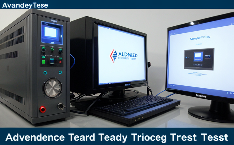
During the testing process, samples are prepared meticulously following standard protocols outlined in ASTM F1385. This includes cleaning processes to eliminate contaminants that could affect measurement accuracy and ensuring specimen orientation is correct for optimal AFM imaging. The testing setup typically consists of an AFM equipped with appropriate tips tailored to specific sample types.
The test procedure involves scanning the prepared surface at specified scan rates, amplitudes, and lateral steps while collecting data points. These raw images are then processed using software that calculates key parameters such as root mean square (RMS) roughness, peak-to-valley height, and mean absolute deviation from planarity.
Results obtained from ASTM F1385 tests play a pivotal role in quality assurance programs by providing quantitative evidence regarding the conformity of manufactured surfaces to specified tolerances. Compliance with these standards ensures consistent performance across batches produced under identical conditions, thereby enhancing reliability and reducing defects in end products.
Incorporating ASTM F1385 into an organization's quality management system can significantly improve product development cycles by identifying potential issues early on through precise surface analysis. It also facilitates better communication between different departments involved in the production process, from R&D to manufacturing, ensuring everyone is aligned towards meeting industry benchmarks.
By leveraging ASTM F1385 micro-roughness testing, companies can maintain their competitive edge in an ever-evolving market where even minor deviations could lead to significant financial losses due to rework or scrapped materials. As technology advances continuously, so too do the requirements placed upon manufacturers; staying ahead of these trends requires robust quality control measures like those provided by ASTM F1385.
To summarize, ASTM F1385 micro-roughness testing serves as a cornerstone for ensuring high-quality semiconductor and microchip manufacturing processes. Its application ensures consistent product performance and reliability while fostering innovation within the industry.
Applied Standards
| Standard Number | Description |
|---|---|
| ASTM F1385 | Standard Practice for Characterization of Surface Roughness by Atomic Force Microscopy (AFM) |
The ASTM F1385 standard is widely recognized and utilized across the semiconductor industry for its precise measurement capabilities. It specifies detailed procedures for preparing samples, conducting AFM scans, analyzing data, and interpreting results.
Adherence to this standard guarantees uniformity in testing protocols among laboratories worldwide, facilitating easier collaboration and comparison of findings between different organizations operating within the sector.
Industry Applications
The application of ASTM F1385 micro-roughness testing extends beyond mere compliance; it plays a vital role in enhancing overall product quality. By meticulously analyzing surface roughness, manufacturers can identify subtle variations that might otherwise go unnoticed during conventional inspection methods.
In semiconductor manufacturing, achieving the desired level of smoothness on surfaces is paramount because even slight imperfections can lead to increased power consumption or reduced efficiency when integrated into circuits. Through rigorous application of ASTM F1385 standards, engineers ensure that every aspect of the production process adheres strictly to predefined limits.
For microchip testing specifically, this method helps manufacturers fine-tune their processes by providing detailed insights into how surface characteristics affect critical parameters like capacitance and resistance values. This knowledge allows them to make informed decisions about design changes or material selections aimed at optimizing performance metrics without compromising on durability or longevity.
In addition to its direct benefits for semiconductor fabrication, ASTM F1385 also supports broader industry goals related to sustainability and environmental responsibility. By promoting efficient use of resources through precise control over manufacturing processes, companies contribute positively towards reducing waste generation throughout the supply chain.
Environmental and Sustainability Contributions
The integration of ASTM F1385 micro-roughness testing into semiconductor production lines not only enhances product quality but also promotes sustainable practices. By minimizing material wastage through accurate measurement techniques, manufacturers can reduce their ecological footprint significantly.
Furthermore, the standard encourages the development of more efficient tools and methodologies for surface characterization, which in turn leads to advancements that benefit both the environment and society at large. For instance, improved understanding of how different materials interact with surfaces allows researchers to explore greener alternatives without sacrificing performance standards.
Through continuous improvement driven by adherence to ASTM F1385 guidelines, the semiconductor industry continues its journey towards becoming more environmentally friendly while maintaining top-tier technological leadership globally.


