ASTM E415 Optical Emission Spectrometry + Microstructure Verification
The ASTM E415 standard optical emission spectrometry (OES) with microstructure verification is a comprehensive analytical service designed to provide detailed chemical and structural insights into metallic materials. This service is particularly valuable for quality managers, compliance officers, R&D engineers, and procurement professionals who need precise characterization of metal alloys.
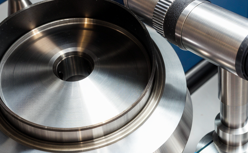
The ASTM E415 method involves the use of an OES instrument, which excites atoms in a sample by passing electrical current through it, causing them to emit light at characteristic wavelengths. This emission is then detected by a spectrometer, allowing for accurate determination of the elemental composition of the material. The service also includes microstructural analysis using scanning electron microscopy (SEM) and energy-dispersive X-ray spectroscopy (EDX), which provide detailed information about the internal structure and phase distribution within the sample.
The combination of OES and SEM/EDX offers a robust approach to metallurgical examination, ensuring precise identification and quantification of alloying elements. This is especially crucial for industries where material quality can significantly impact product performance and safety. For instance, in aerospace applications, understanding the exact composition of alloys like aluminum or titanium is critical for optimizing strength-to-weight ratios.
Compliance officers will find this service invaluable when ensuring that materials meet stringent industry standards such as ASTM E415 itself, as well as other relevant international specifications. R&D engineers can leverage these results to refine material formulations and improve product performance. In procurement, the detailed reports generated by this service help in verifying supplier claims about material quality.
The accuracy of OES measurements is enhanced by meticulous sample preparation techniques that include cleaning, pickling, and etching processes tailored for different metals. These steps ensure that the surface of the specimen reflects true internal composition without interference from contaminants or external layers. SEM/EDX analysis further supports this by providing high-resolution images and elemental mapping capabilities.
The analytical process begins with selecting appropriate samples representative of the batch or lot being tested, followed by thorough cleaning to remove oxides and other impurities. The cleaned sample is then placed into the OES instrument where it undergoes excitation and emission detection. Afterward, SEM/EDX is employed for microstructural examination.
The resulting data from both OES and SEM/EDX analyses are compiled into comprehensive reports that serve as definitive evidence of material quality. These reports include detailed tables listing detected elements along with their concentrations, accompanied by visual representations such as images captured during the analysis process. Such documentation is essential for regulatory compliance, internal audits, and supplier evaluations.
By offering ASTM E415 optical emission spectrometry coupled with microstructure verification, our laboratory ensures that clients receive reliable, accurate information about their materials. This service supports decision-making processes related to material selection, quality assurance, and process optimization across various sectors including aerospace, automotive, electronics, and manufacturing.
Why It Matters
The importance of ASTM E415 optical emission spectrometry cannot be overstated in the context of metallurgy and material testing. This method plays a vital role in ensuring that materials used across industries meet specific chemical composition requirements set forth by standards organizations like ASTM.
Accuracy is paramount when dealing with complex alloys where even minor variations in elemental content can lead to significant differences in mechanical properties or performance characteristics. For example, in the production of stainless steel, precise control over nickel and chromium concentrations ensures resistance to corrosion while maintaining strength and ductility. In titanium alloys used in medical implants, accurate quantification of vanadium helps optimize bone integration.
From a regulatory perspective, compliance with ASTM E415 is crucial for manufacturers looking to avoid costly recalls or legal actions stemming from non-conforming products. By adhering strictly to these standards during production processes, companies can maintain high standards of quality and reliability in their offerings.
In terms of safety considerations, especially in sectors like aerospace where human lives depend on the integrity of materials used, it is imperative that every batch undergoes rigorous testing using methods such as those prescribed by ASTM E415. This not only protects end users but also builds trust among stakeholders who rely on consistent performance from suppliers.
The ability to accurately identify and quantify alloying elements through OES analysis allows for better control over production processes, leading to improved efficiency and reduced waste. Additionally, the detailed microstructural information obtained via SEM/EDX can guide modifications aimed at enhancing specific material properties without compromising overall quality or cost-effectiveness.
In summary, ASTM E415 optical emission spectrometry serves as an indispensable tool for ensuring that materials used in critical applications meet stringent requirements set by industry standards. Its significance lies not only in meeting regulatory expectations but also in enabling continuous improvement through informed decision-making based on precise analytical data.
Benefits
The benefits of utilizing ASTM E415 optical emission spectrometry for metallographic examination and microstructure analysis are numerous and far-reaching. One key advantage is the ability to achieve high accuracy in determining elemental compositions, which is essential for ensuring compliance with international standards such as those set by ASTM.
For quality managers, this service provides peace of mind knowing that their products meet strict chemical specifications, thereby reducing risks associated with non-compliance issues. Compliance officers can rely on these results to verify supplier claims and maintain consistent product quality throughout supply chains. R&D engineers benefit from detailed insights into material behavior under various conditions, which aids in optimizing designs and improving performance.
From an operational standpoint, the precision offered by ASTM E415 helps minimize errors during production processes, leading to increased efficiency and reduced waste. In industries where safety is paramount, such as aerospace or medical devices, ensuring that materials comply with relevant standards enhances reliability and trustworthiness among stakeholders.
The use of SEM/EDX in conjunction with OES analysis offers additional value by providing detailed microstructural information about the internal structure of materials. This capability enables manufacturers to make informed decisions regarding process improvements aimed at enhancing specific material properties without compromising overall quality or cost-effectiveness.
Another significant benefit is the ability to detect trace elements that may have an impact on the performance or longevity of a particular alloy. For instance, in stainless steel production, detecting even small amounts of sulfur can indicate potential issues related to hot cracking during casting processes. Identifying such impurities early allows for corrective actions before they become costly problems down the line.
In summary, ASTM E415 optical emission spectrometry provides a comprehensive approach to material analysis that offers multiple advantages across different aspects of industrial operations. Its focus on accuracy, precision, and compliance supports quality assurance efforts while fostering innovation through deeper understanding of materials behavior.
Use Cases and Application Examples
| Material Type | Application | ASTM E415 OES + SEM/EDX Benefits |
|---|---|---|
| Aerospace Alloys (e.g., Titanium, Aluminum) | Making sure parts are safe and reliable for use in aircraft structures. | Detecting trace impurities that could lead to fatigue cracks or corrosion issues. |
| Medical Devices (e.g., Stents, Implants) | Ensuring biocompatibility of materials used in contact with human tissues. | Identifying alloy components that ensure proper biological response and durability. |
| Automotive Steels | Optimizing fuel efficiency by selecting lightweight yet strong materials. | Evaluating carbon content to balance strength and formability during cold forming processes. |
| Electronics Grade Copper | Guaranteeing purity levels meet stringent specifications for electrical conductivity. | Determining copper concentration accurately while also examining grain structure for optimal heat treatment. |
| Industrial Grades of Stainless Steel | Maintaining consistent quality across batches to ensure product reliability and customer satisfaction. | Monitoring nickel, chromium, molybdenum levels consistently to maintain desired corrosion resistance properties. |
The use cases for ASTM E415 optical emission spectrometry with microstructure verification are extensive across various industries. In aerospace alloys like titanium and aluminum, detecting trace impurities that could lead to fatigue cracks or corrosion issues is crucial for ensuring the safety and reliability of parts used in aircraft structures. For medical devices such as stents and implants, it's essential to ensure biocompatibility by identifying alloy components that will have a proper biological response and durability.
In automotive steels, optimizing fuel efficiency by selecting lightweight yet strong materials is achieved through evaluating carbon content which balances strength and formability during cold forming processes. For electronics grade copper, guaranteeing purity levels meet stringent specifications for electrical conductivity requires determining copper concentration accurately while examining grain structure for optimal heat treatment.
Industrial grades of stainless steel must maintain consistent quality across batches to ensure product reliability and customer satisfaction. Monitoring nickel, chromium, molybdenum levels consistently ensures desired corrosion resistance properties are achieved. These examples illustrate how ASTM E415 optical emission spectrometry with microstructure verification plays a critical role in various applications within different sectors.


